Full Stack Electronics · Stage Three · Experiment 9
Make both of the 555's references on the board from three equal resistors. Then lower the supply and measure how they follow it.
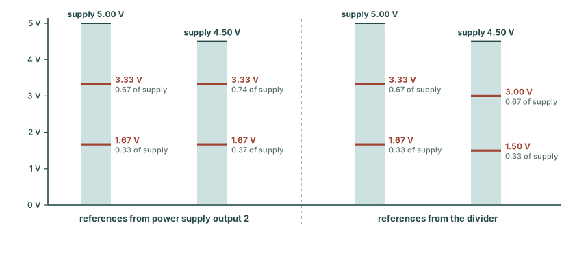
Experiments 7 and 8 tested each comparator against power supply output 2, set by hand to 3.33 V or 1.67 V. That was a temporary reference. Inside the 555, three equal resistors run in series from the supply pin to ground. The upper join between them sits at 2/3 of the supply and is the threshold comparator's reference. The lower join sits at 1/3 and is the trigger comparator's reference. A chain like this is called a voltage divider. Both references are fixed shares of the supply, so they follow it when it changes, as Figure 9-1 shows. That keeps the 555's timing the same at any supply. In the finished 555 the timing capacitor charges from 1/3 to 2/3 of the supply, and that climb takes the same time whatever the supply is. The theory box “Why the timing ignores the supply” explains this. It comes after the tap readings. This experiment builds the divider, measures it at 5.00 V and 4.50 V, and connects it to both comparators.
Before the divider goes on the board, here is how three resistors make the two references. Figure 9-2 is the circuit. R1, R2 and R3 are 10 kΩ resistors in series from +5 V to ground. A tap is a join between two resistors where a voltage is taken off: the 2/3 tap between R1 and R2, and the 1/3 tap between R2 and R3.
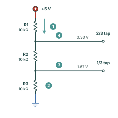
At 4.50 V each resistor drops 1.50 V, and the taps move to 3.00 V and 1.50 V. The shares depend only on how the three resistances compare, so the three have to match. Their common value sets two smaller things: the current through the chain, and how far a tap's voltage moves when something draws current from it. Later in this experiment each comparator input draws a few microamps from its tap. With 10 kΩ resistors that moves a tap by a few tens of millivolts, and Figure 9-7 shows that shift.
The NE555's divider uses 5 kΩ for each of its three resistors, half the value on this board. Several books say the chip takes its name from them: 5, 5, 5. Its designer said otherwise. Hans Camenzind designed the 555 for Signetics, and in an oral-history interview for the Transistor Museum he said the number was chosen arbitrarily. Art Fury, Signetics' marketing manager, expected the circuit to sell well and picked "555" from the company's 500 series of part numbers. The three resistors do have the same value, and the match with the name is a coincidence.
The divider replaces power supply output 2, so the bench connections from Experiment 8 come off first. That experiment left power supply output 2 and the generator on the threshold comparator, each lead clipped onto a 1 kΩ resistor.
Figure 9-2 draws the divider with +5 V at the top. The +5 V rail of this board is at the bottom, so on the board the divider stands upside down. It goes in column 15, between the two comparators. That column is free in both blocks, so R2 can cross the centre channel. The lower strip of column 15 (rows f to j) becomes the 2/3 tap, and the upper strip (rows a to e) the 1/3 tap. Figure 9-3 shows the divider and where the multimeter goes.
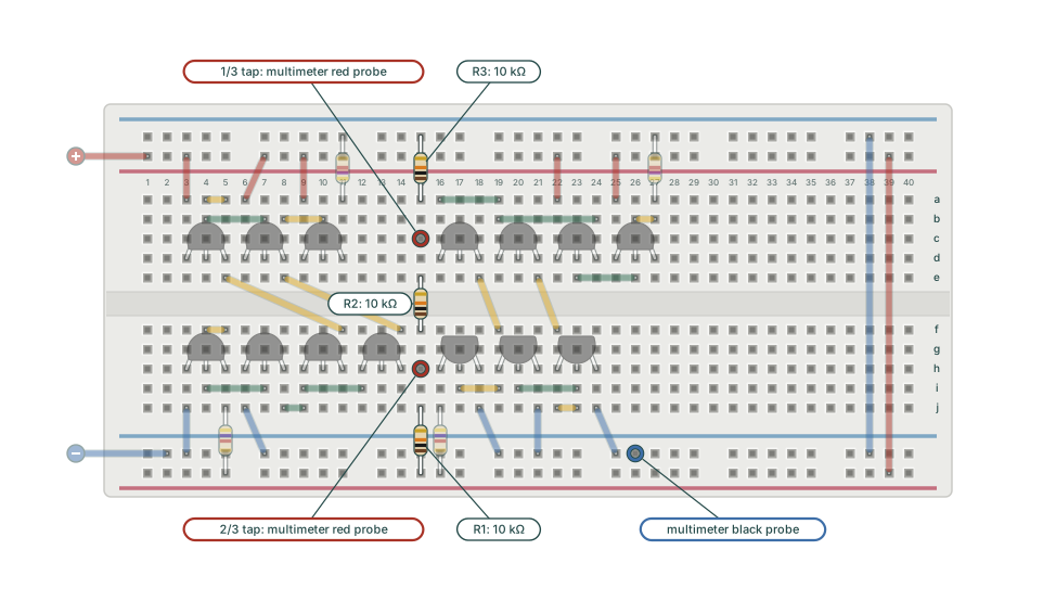
The divider is complete, and nothing takes current from its taps yet. The taps are shares of the voltage that reaches the board, so set the supply by the multimeter.
If both taps read close to 0 V, R1 is on the inner bottom rail, which is ground. If both read close to the supply, R3 is on the inner top rail, which is +5 V. Switch off and move that resistor's lead to the outer rail.
The table gives the expected values and the readings from my first build of this circuit. The number in brackets beside each reading is that reading divided by the supply.
| Supply | 2/3 tap, expected | 2/3 tap, my first build | 1/3 tap, expected | 1/3 tap, my first build |
|---|---|---|---|---|
| 5.00 V | 3.333 V | 3.354 V (0.671) | 1.667 V | 1.695 V (0.339) |
| 4.50 V | 3.000 V | 3.018 V (0.671) | 1.500 V | 1.525 V (0.339) |
Both taps fell with the supply and kept their share: 0.671 and 0.339 at both supplies. The small offset from 0.667 and 0.333 is the three resistors differing by a fraction of a percent. Set the supply back to 5.00 V, measured on the bottom +5 V rail.
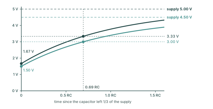
The table showed both taps keeping their share of the supply. Here is why that keeps the 555's timing the same. In the finished 555, a resistor charges the timing capacitor from the supply, and the capacitor's voltage climbs from the 1/3 tap to the 2/3 tap. The current through the resistor depends on the voltage across it: the supply minus the capacitor's voltage. Call that the gap. On a 5.00 V supply the gap starts at 3.33 V and ends at 1.67 V. On 4.50 V it starts at 3.00 V and ends at 1.50 V. On both supplies the climb ends when the gap has halved.
As the gap shrinks, the current shrinks with it, so the gap falls by the same fraction in each equal stretch of time, like a half-life. Halving takes the same time whatever size the gap starts at: 0.69 RC on both supplies, as Figure 9-4 shows. With references fixed at 3.33 V and 1.67 V on a 4.50 V supply, the gap would fall from 2.83 V to 1.17 V, which is less than half, and the climb would take 28 % longer.
Call the supply , the capacitor's voltage , and the gap between them :
The current through the resistor is the gap divided by the resistance. All of it flows into the capacitor, and a current into a capacitor raises its voltage at a rate of current divided by capacitance:
The supply does not change, so the gap shrinks exactly as fast as the capacitor's voltage rises:
A quantity that shrinks at a rate proportional to its own size decays exponentially. If the gap is at the start, then after a time it is
The climb ends when the gap has fallen to . Divide both sides by to get
and take the natural logarithm of both sides:
The time depends only on the ratio of the two gaps. With the divider, the climb starts at and ends at :
The supply cancels in the ratio:
With references fixed at 1.67 V and 3.33 V on a 4.50 V supply, the gaps are
so the climb takes
That is 0.887 / 0.693 = 1.28 times the time with the divider: 28 % longer. The 0.693 is the number in the NE555's timing formula in Experiment 1.
The divider makes both references, and they follow the supply. It can now replace power supply output 2 at both comparators. In the finished 555, each comparator compares its reference with the timing capacitor's voltage. Experiment 12 adds the capacitor. Until then a triangle from the generator stands in for the capacitor's voltage, and this page calls it the ramp.
Which input takes the ramp depends on the latch. The latch of Experiment 11 is switched by high levels, so each comparator's OUT has to go high when the ramp leaves the band between the taps: the threshold comparator's above 2/3, the trigger comparator's below 1/3. Experiments 7 and 8 measured both comparators with OUT high while V+ is below V−. The trigger comparator keeps the ramp on V+ and takes the 1/3 tap on V−, so its OUT is high while the ramp is below 1/3. The threshold comparator needs its inputs swapped from Experiment 7: the 2/3 tap goes on V+ and the ramp on V−, so its OUT is high while the ramp is above 2/3. Figure 9-5 draws both.
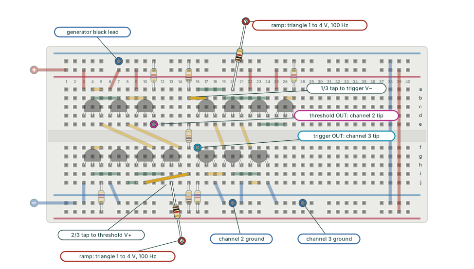
The ramp reaches each comparator through its own 1 kΩ, as in Experiments 7 and 8, because a base at the end of an instrument's lead can oscillate. The taps reach their bases on short jumpers and need no resistor.
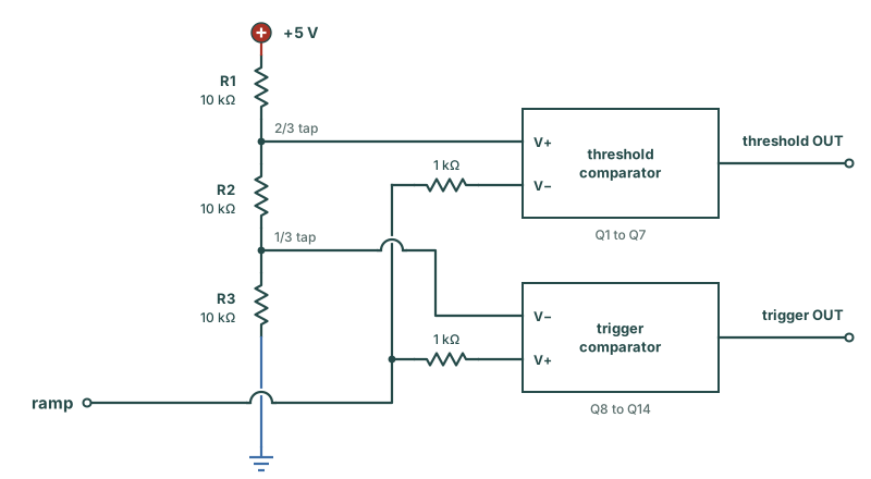
Figure 9-6 shows those connections on the board. The 2/3 tap reaches Q1's base at 10j on a diagonal jumper from 15i, and the 1/3 tap reaches Q9's base on a short jumper from 15b to 17b. The trigger's 1 kΩ stands in 20a, Q8's base column, as in Experiment 8. The threshold's 1 kΩ stands in 13j, Q2's base column, as in Experiment 7. The ramp goes to the free leg of each, and Figure 9-6 gives both free legs the same label.
If a comparator switches near the other comparator's reference, its tap jumper is in the wrong strip of column 15. The 2/3 tap is the lower strip, rows f to j. The 1/3 tap is the upper strip, rows a to e. If the threshold comparator's OUT is high while the ramp is low, its inputs are the Experiment 7 way round: check that the 2/3 jumper ends in 10j and the 1 kΩ stands in 13j.
Both comparators now take their references from the divider and share one ramp. Together they are the 555's analogue front end, all made from the 5 V supply. The threshold comparator's OUT should be high while the ramp is above 3.33 V, and the trigger comparator's while it is below 1.67 V.
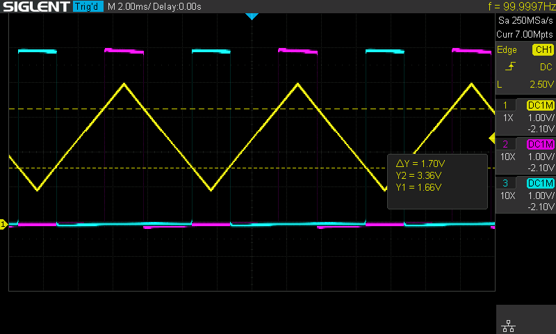
The two outputs are high at opposite ends of the ramp, and both are low between the taps. In the finished timer, the capacitor moves only in that band, and the two high levels at its edges are what Experiment 11's latch needs. The switching points can sit a few tens of millivolts from the tap readings in the table. Each comparator input now draws a few microamps from its tap, and with 10 kΩ resistors that moves the tap by a few tens of millivolts.
The tap measurements showed the divider following the supply on its own. The last measurement checks the same with the comparators connected: at 4.50 V the switching points should move with the taps, to 3.00 V and 1.50 V.
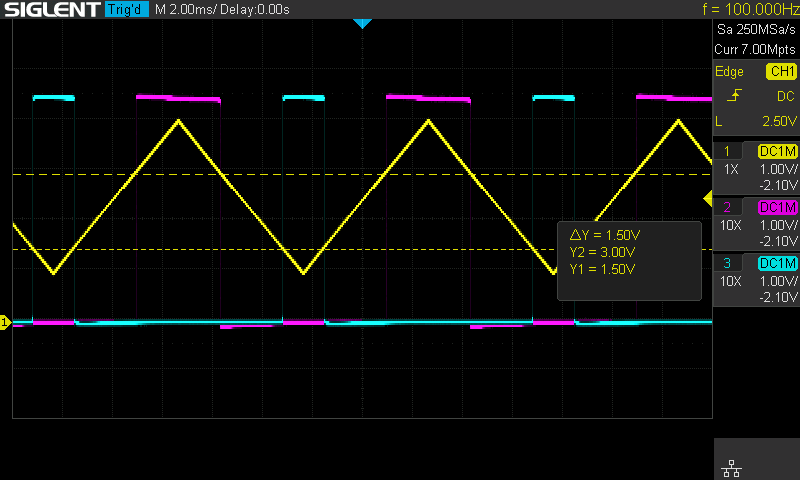
Figure 9-8 shows both switching points moving down with the taps. Set the supply back to 5.00 V when you have finished.
No flaw joins the list. Every flaw on it is fixed or reduced.
| # | Flaw | What it means | Found | Status |
|---|---|---|---|---|
| 1 | No reference input | The threshold is the transistor's own 0.6 V. Nothing outside the circuit sets it. | Experiment 3 | Fixed in Experiment 4: the differential pair |
| 2 | Wide transition | The output needs a band of input to travel from high to low: about half a volt with one transistor, about a quarter of a volt with the pair. | Experiment 3 | Fixed in Experiment 6: the active load |
| 3 | Thermal drift | The base-emitter voltage falls about 2 mV per degree, and the threshold falls with it. | Experiment 3 | Reduced in Experiment 4: two matched transistors drifting together |
| 4 | Tail current follows the common-mode level | A resistor tail passes more current as both inputs rise, and the output moves with it. | Experiment 4 | Fixed in Experiment 5: the current mirror tail |
| 5 | Output low trapped a diode drop below the reference | The output's low level sits a diode drop below the reference instead of at ground. | Experiment 6 | Fixed in Experiment 7: the PNP output stage |
Three questions on this experiment: what the divider's resistors must have in common, what the taps do when the supply falls, and why the threshold comparator's inputs were swapped.
1. The divider's three resistors have to match because…
The same current flows through all three. Equal resistors drop equal voltages, so the taps sit at exactly 1/3 and 2/3 of the supply. The common value sets the current and how far a small load moves a tap, but it does not change the shares.
2. The supply falls from 5.00 V to 4.50 V. The taps…
Each tap is a fixed share of the supply. At 4.50 V, 2/3 is 3.00 V and 1/3 is 1.50 V. A reference set on power supply output 2 would have stayed at 3.33 V and 1.67 V.
3. The threshold comparator takes the 2/3 tap on V+ and the ramp on V− because…
Both comparators have OUT high while V+ is below V−. With the tap on V+, the threshold comparator's OUT goes high when the ramp rises above 2/3, which is the signal the latch needs. The trigger comparator keeps the ramp on V+, so its OUT is high below 1/3.
Three matched resistors replaced power supply output 2. Their taps keep their share of the supply, so the 555's timing stays the same at any supply. The board now carries the 555's analogue half: the divider and both comparators.
Neither output remembers anything. When the ramp leaves the bottom of the band, the trigger comparator's OUT falls again, but the capacitor has to keep charging until it reaches 2/3. So the 555 needs one bit of memory that records which comparator was high last. That memory is a latch made of two logic gates. Experiment 10: The NOR Gate builds the gate from transistors, and Experiment 11 joins two of them into the latch.