Full Stack Electronics · Stage Three · Experiment 10
Build the gate of the timer's memory from two transistors and three resistors. Then measure its output for all four combinations of its inputs.
Experiment 9 connected both comparators to the divider and to one ramp. Each comparator's OUT goes high while the ramp is outside the band between the taps, and falls as soon as the ramp comes back inside. In the finished timer the capacitor must keep charging after the trigger comparator's OUT falls, until it reaches 2/3 of the supply. So the timer needs one bit of memory that records which comparator was high last.
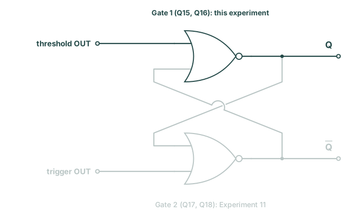
In Experiment 2 that memory was a latch made from two NOR gates in a CD4001B chip. A NOR gate's output is high only when both of its inputs are low. This experiment builds one NOR gate from two 2N3904 transistors and three resistors, and measures it. Experiment 11 builds the second gate and joins the two into the latch. Figure 10-1 shows where this gate goes.
The NOR gate starts from a circuit that this course built in Experiment 3: the transistor switch. One 2N3904 has a 10 kΩ resistor into its base, a 1 kΩ resistor from its collector to +5 V, and its emitter on ground. The collector is the output. Experiment 3 tested this switch as a comparator and found three flaws. Its output fell over a band of input from 0.60 V to 1.10 V. The transistor itself set where that band starts, and the band moved when the transistor became warm.
A logic circuit uses the same switch in a different way. In this course a 0 is a voltage near 0 V and a 1 is a voltage near +5 V, as in Experiment 2. A logic input sits at one of those two levels, and the band is far from both. Figure 10-2 shows the switch's output for every input from 0 V to 5 V. A 0 can rise by 0.6 V before the output starts to fall, and a 1 can drop by 3.9 V. In Experiment 3 a heat gun moved the band by 0.26 V, which is less than either of those.
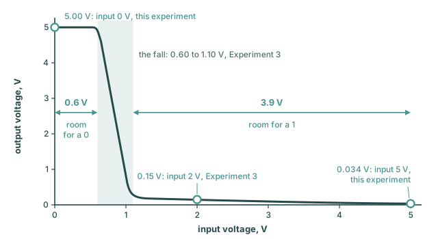
So a 0 at the input gives a 1 at the output, and a 1 gives a 0. A circuit that does this is an inverter, also called a NOT gate. The three flaws that matter in a comparator do not change the output of an inverter, because its input stays out of the band.
An inverter has one input, and each gate of the latch needs two. The second input gets its own transistor. Put a second 2N3904 beside the first, with its collector on the same collector line and its emitter on the same ground. Give it its own 10 kΩ and its own input. Figure 10-3 shows the result: Q15 takes input A, Q16 takes input B, and both share the 1 kΩ pull-up and OUT. The name pull-up says what the resistor does: it pulls OUT up to +5 V while neither transistor conducts.
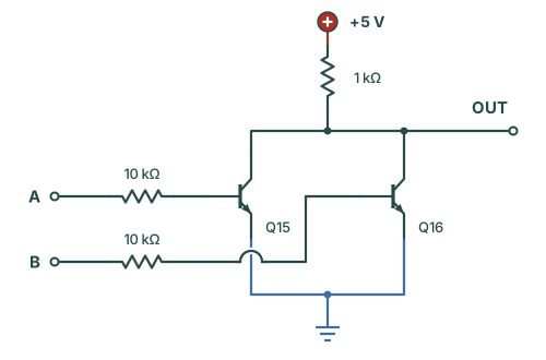
Figure 10-4 draws the same circuit four times, once for each combination of the two inputs. A transistor that is off is pale, and green arrows show where current flows. The list gives the reason for each panel, in the same order.
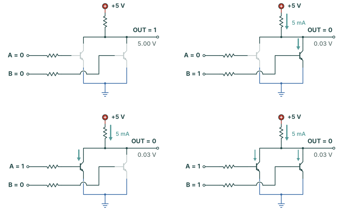
So OUT is a 1 only when A and B are both 0. That is the NOR rule from Experiment 2. Without the inversion it would be the OR rule: high when A or B is high. Remove Q16, and the circuit is the inverter again.
The gate goes in the lower block, right of the trigger comparator, in columns 28 to 33. Its emitters go on the inner bottom rail, which is ground. So the transistors stand in row h with their flat faces towards the far edge, like Q12 to Q14. Each input is a 10 kΩ from its transistor's base down to the bottom rails. The rail that holds its lower leg sets the input. The inner bottom rail is ground, a 0, and the outer bottom rail is +5 V, a 1. Nothing crosses the centre channel, so the upper block above the gate stays empty. Experiment 11 puts the second gate there, straight above this one.
Experiment 9 left the generator, the crocodile-clip lead and two oscilloscope probes on the comparators, so those come off first. The two 1 kΩ ramp resistors in 13j and 20a stay. Figure 10-5 shows the finished gate and where the multimeter goes.
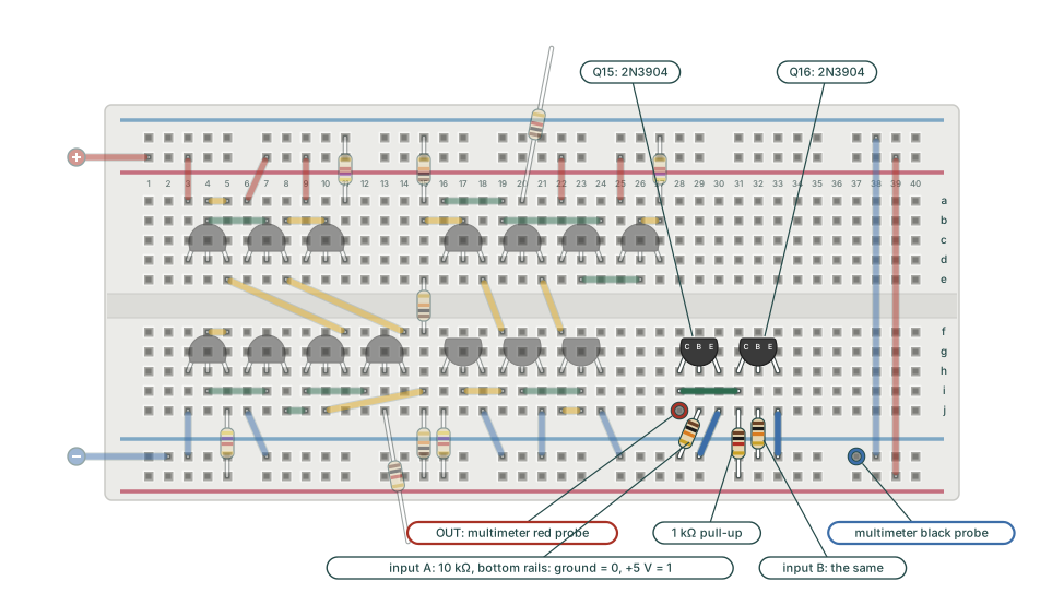
Always set an input through its 10 kΩ. A wire from +5 V straight to a base puts the base-emitter junction directly across the supply. The supply then reaches its 50 mA current limit, the +5 V rail falls for the whole board, and the transistor can be damaged.
The gate is complete, with both inputs at 0. The multimeter now reads OUT for each combination of Figure 10-4. Expect about 5.00 V for the first combination and a few hundredths of a volt for the other three.
If OUT stays near 0 V with both inputs at 0, check the input resistors. The lower leg of each must be in the inner bottom rail. Also check that each transistor has its flat face towards the far edge. If OUT stays near 5 V with an input at 1, check that the pull-up goes to the outer bottom rail. Both emitter jumpers must go to the inner bottom rail.
The table gives the expected values, the readings from my first build of this gate, and two readings from my current board. Figures 10-6 and 10-7 show the multimeter for these two readings.
| A | B | On | OUT | Expected | My first build | My current board |
|---|---|---|---|---|---|---|
| 0 | 0 | neither | 1 | 5.00 V | 5.001 V | 5.003 V |
| 0 | 1 | Q16 | 0 | 0.03 V | 0.034 V | not measured |
| 1 | 0 | Q15 | 0 | 0.03 V | 0.034 V | 0.050 V |
| 1 | 1 | both | 0 | 0.03 V | 0.034 V | not measured |
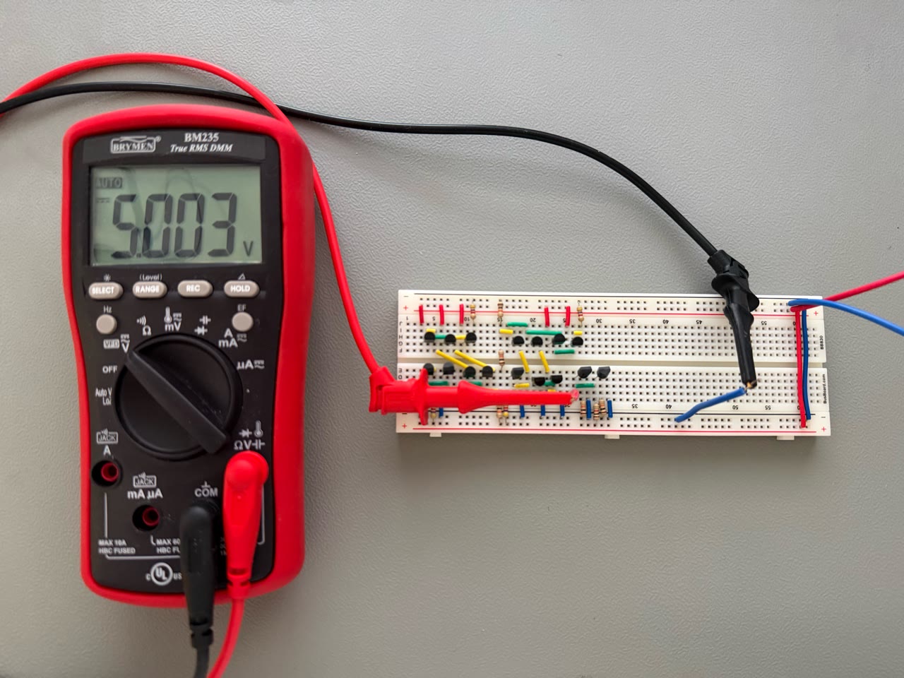
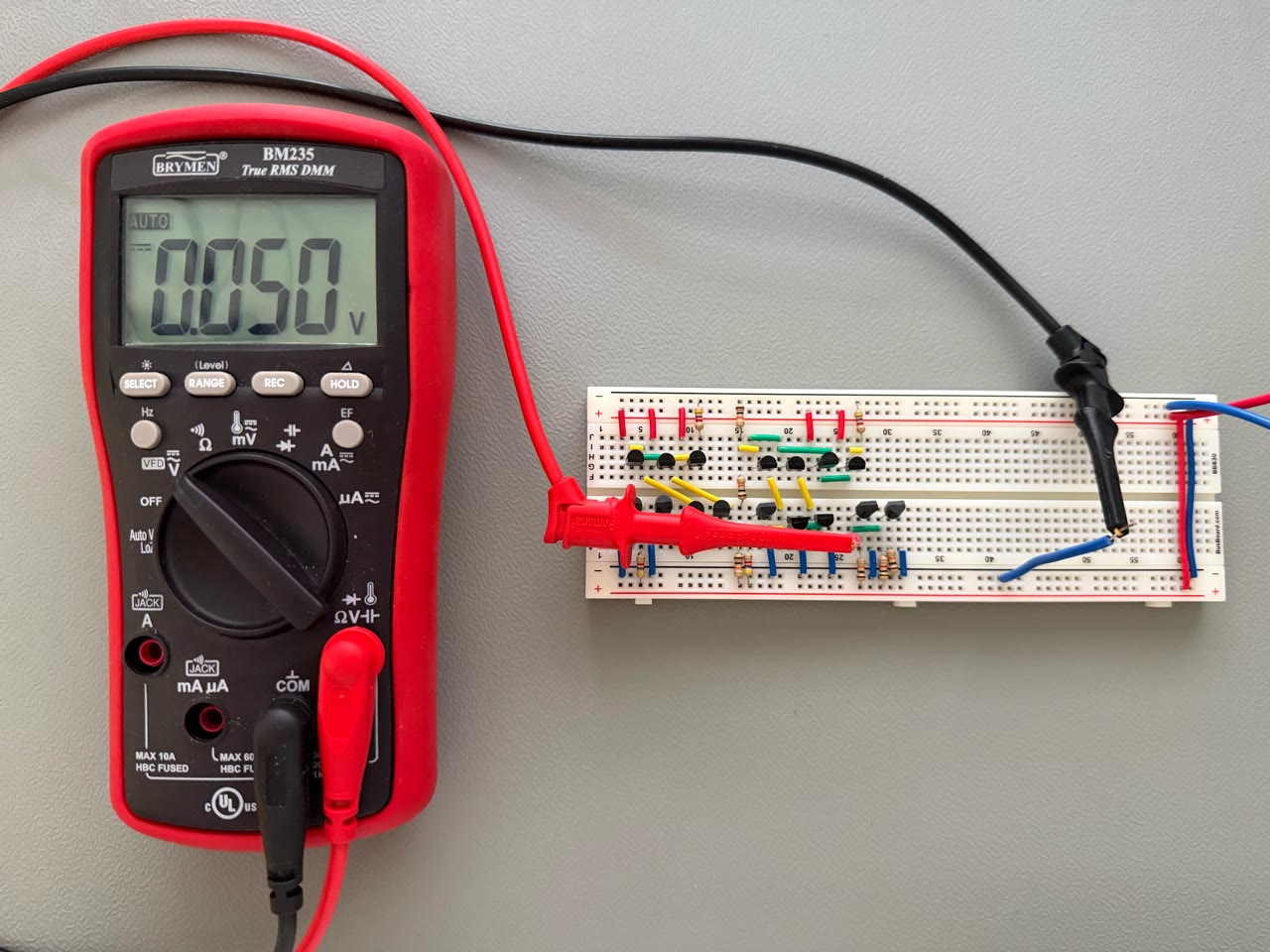
OUT is a 1 only with both inputs at 0, so the gate follows the NOR rule. The 1 is within a few millivolts of 5 V on both boards: with both transistors off, almost no current flows through the 1 kΩ. On my first build the 0 read 0.034 V in all three combinations with an input at 1. On my current board it read 0.050 V with A at 1. Both are lower than the 0.15 V that Experiment 3 measured on the same switch, and the next section explains the difference.
A transistor that is fully on is saturated, as Experiment 3 described. Its low level depends on how much base current it gets, compared with the base current that its collector current needs.
Experiment 3 drove the same switch from a 2 V input. That gave (2.0 V − 0.7 V) / 10 kΩ = 0.13 mA of base current and a low of 0.15 V. The gate's 5 V input gives more than three times that base current, and the low falls to 0.034 V. A low this close to 0 V is useful in Experiment 11, where the OUT of one gate drives an input of the other. Figure 10-2 shows that a 0 at 0.034 V is far below the 0.6 V where the next transistor starts to conduct.
The list under “Why the low is 0.034 V” said that extra base current pushes the transistor further into saturation. Here is what happens inside it. A transistor is saturated when both of its junctions conduct: base to emitter, and base to collector. The collector-to-emitter voltage is then the difference between the two junction voltages:
With barely enough base current, the base-collector junction conducts only a little. Its voltage is well below the base-emitter voltage, and the difference is a few tenths of a volt. More base current makes the base-collector junction conduct harder, and its voltage comes closer to the base-emitter voltage. The difference then shrinks to a few tens of millivolts. With both inputs at 1, each transistor gets the same base current and carries only part of the 5 mA. So each one is at least as far into saturation as a single transistor, and the low cannot rise. On my first build it read 0.034 V in all three combinations.
The multimeter showed the four combinations one at a time. The oscilloscope shows the gate following an input that changes. The generator drives input A with a square wave from 0 V to 5 V, and input B stays at 0. Figure 10-8 shows the connections. Oscilloscope channel 1 still shows the generator's signal through the BNC T-piece, as in Experiment 9.
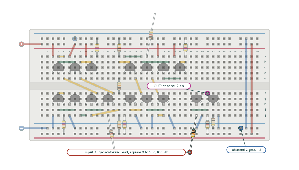
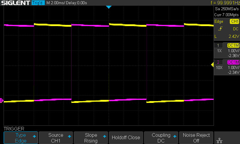
With B at 0, the gate is an inverter: OUT is high while A is low, and low while A is high. Now set B to 1 while A keeps switching.
With B at 1, OUT stays low and the square wave on A has no effect. One input at 1 is enough to hold OUT low, whatever the other input does. That is the OR in the NOR rule.
NOR gates alone can make any logic function: NOT, OR, AND, and also memory. The Apollo Guidance Computer, which steered the Apollo spacecraft to the Moon, used that fact. It was one of the first computers made from integrated circuits. The version that flew used about 2,800 identical chips, each with two three-input NOR gates. Each of those gates had the form of Figure 10-3 with a third transistor. This kind of logic is called resistor-transistor logic, often shortened to RTL.
RTL has two weak points. A saturated transistor takes time to turn off, because its base has to lose the extra charge that saturation put there. And the 1 comes only through a pull-up resistor, so one output can drive only a few inputs. Later logic families, first TTL and then CMOS, replaced RTL for those reasons. Neither weak point matters in this timer. Its latch changes state at the speed of a charging capacitor, and each gate output drives only a few inputs.
Three questions on this experiment. They ask when OUT is high, what happens with both inputs at 1, and why the switch's flaws from Experiment 3 do not matter in a gate.
1. OUT is near +5 V only when…
The pull-up holds OUT at +5 V only while no current flows through it. That needs both transistors off, so both inputs at 0. One input at 1 turns its transistor on, and OUT falls to a few hundredths of a volt.
2. With both inputs at 1, OUT…
One saturated transistor already holds OUT a few tens of millivolts above ground. A second one in parallel shares the current and cannot take OUT below ground. My first build read 0.034 V for one input at 1 and for both.
3. The switch from Experiment 3 has a wide transition that moves with temperature. In a gate this does not change the output, because…
The output falls only for inputs between about 0.60 V and 1.10 V. A 0 has 0.6 V of room below that band and a 1 has 3.9 V above it. The heat gun moved the band by 0.26 V, which is less than either.
Two transistors, a shared 1 kΩ pull-up and two 10 kΩ resistors make a NOR gate. Its 1 is 5.00 V and its 0 is 0.034 V, both far from the band where the switch changes state. The gate stays on the board, in columns 28 to 33.
The gate still remembers nothing: OUT follows its inputs at every moment. Experiment 11: The SR Latch builds a second gate above this one and connects each gate's OUT to an input of the other. The pair then keeps its state after the input that set it returns to 0.