Full Stack Electronics · Stage Three · Experiment 8

Experiment 8: The PNP Twin

Build the 555's second comparator from the other kind of transistor. Then measure how close to ground the first one keeps working.

The comparator finished in Experiment 7 is the 555's threshold comparator. It watches for the timing capacitor to rise past 2/3 VCC, 3.33 V on a 5 V supply. The 555 has a second comparator, the trigger comparator. It watches for the capacitor to fall below 1/3 VCC, 1.67 V, and starts the next cycle. Its input falls towards ground, so this comparator has to work closer to 0 V than the threshold comparator.

In Ken Shirriff's analysis of the NE555's die, the threshold comparator has NPN input transistors and the trigger comparator has PNPs. The probable reason is where each pair's emitters sit. An NPN pair holds its emitters a base-emitter drop below its inputs, and its tail needs room between them and ground. Experiment 7 measured the NPN pair's low level at 1.12 V with V− at 1.67 V, so its emitters already sit about 1 V above ground. As both inputs fall towards ground, that room runs out. A PNP pair holds its emitters a drop above its inputs, and its tail hangs from +5 V, where the room stays.

So this experiment builds the trigger comparator. It is the circuit of Experiment 7 with every NPN swapped for a PNP, every PNP for an NPN, and +5 V and ground exchanged. Its 1.67 V reference comes from power supply output 2. The first measurements check that it switches at 1.67 V with its output at 0 V and 5 V. Then the floor test lowers the threshold comparator's reference towards ground and measures where the NPN pair stops working.

You will need

The same comparator, turned over

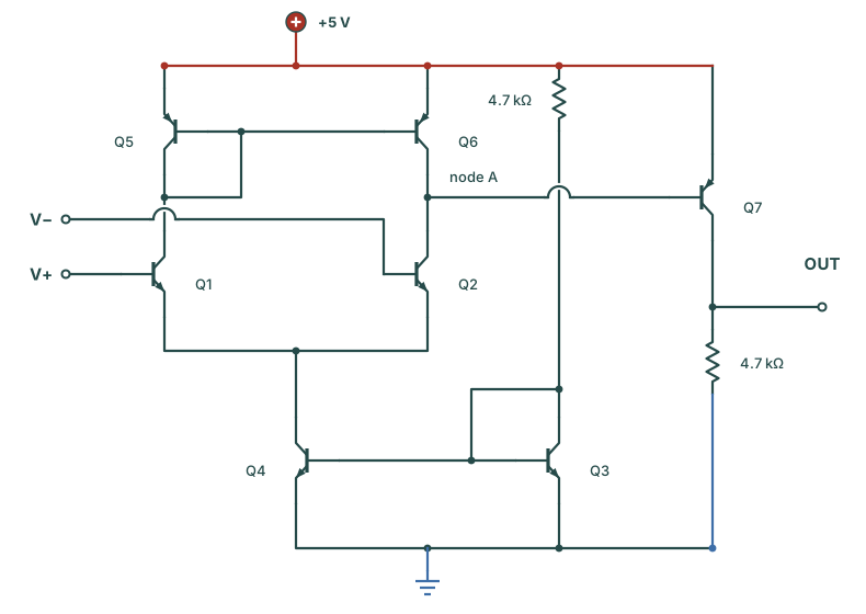
The plan is to swap every transistor for the other kind and exchange the rails. To see what that does to each stage, start from the circuit as Experiment 7 finished it. Figure 8-1 is the whole threshold comparator. The NPN pair Q1 and Q2 has the NPN tail mirror Q3 and Q4 below it, and the PNP mirror Q5 and Q6 above it as the load. The PNP output stage Q7 reads node A from the +5 V line.

Schematic of the threshold comparator. A +5 volt line along the top feeds the emitters of the PNP mirror Q5 and Q6, the emitter of Q7, and a 4.7 kilohm resistor at the far right. Q5's collector is joined to its base. Below the mirror is the NPN pair Q1 and Q2, with V+ on Q1's base, V− on Q2's base and the emitters joined. Below the pair is the NPN tail mirror Q3 and Q4, with its emitters on ground. Q3 stands to the right of Q4, fed by that 4.7 kilohm resistor, with its collector joined to its base. Q4's collector feeds the pair's emitters. Node A, Q2's collector, runs to Q7's base. Q7's collector is OUT, with a 4.7 kilohm resistor to ground.
Figure 8-1: The threshold comparator as Experiment 7 finished it. The input pair and its tail are NPN, next to ground. The load and the output stage are PNP, next to +5 V.

Figure 8-2 is the trigger comparator, drawn on the same skeleton. Each stage moves to the other rail, and +5 V stays at the top of the drawing. Q10 is drawn to the right of Q11, where it stands on the board. The seven transistors are numbered on from the threshold comparator's, Q8 to Q14. Each number is seven more than the transistor it replaces: Q8 does Q1's job, and Q14 does Q7's.
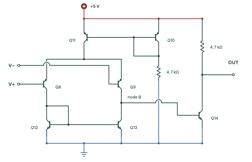
Schematic of the trigger comparator. A +5 volt line along the top feeds the emitters of the PNP tail mirror, Q11 above the pair and Q10 to its right, and a 4.7 kilohm pull-up at the far right. Q10's collector is joined to its base and runs through a 4.7 kilohm resistor to ground. Q11's collector feeds the joined emitters of the PNP pair Q8 and Q9 below it, with V+ on Q8's base and V− on Q9's base. Below the pair is the NPN load Q12 and Q13, with its emitters on ground. Q12's collector is joined to its base. Node B, Q9's collector, runs to the base of Q14, an NPN with its emitter on ground. Q14's collector is OUT, pulled up to +5 volts through the 4.7 kilohm resistor.
Figure 8-2: The trigger comparator. The input pair and its tail are PNP, hanging from +5 V. The load and the output stage are NPN, standing on ground. Q9's collector is the comparator's output node, node B.

Put Figure 8-2 beside Figure 8-1. Each stage has its opposite number on the other rail:

StageThreshold comparator (Figure 8-1)Trigger comparator (Figure 8-2)
Input pairQ1, Q2: NPN, emitters joined below themQ8, Q9: PNP, emitters joined above them
Tail mirrorQ3, Q4: NPN, emitters on ground, 4.7 kΩ from +5 VQ10, Q11: PNP, emitters on +5 V, 4.7 kΩ to ground
LoadQ5, Q6: PNP mirror on +5 VQ12, Q13: NPN mirror on ground
Output nodenode A, Q2's collectornode B, Q9's collector
Output stageQ7: PNP, emitter on +5 V, 4.7 kΩ pull-downQ14: NPN, emitter on ground, 4.7 kΩ pull-up

Current still flows from +5 V to ground, but each stage now handles it from the other side. In the threshold comparator, the tail mirror stands below the pair and draws the tail current out of its emitters to ground. In the trigger comparator, the tail mirror hangs above the pair and pushes the tail current into its emitters from +5 V. The voltage limits also reverse, and the node B check measures that.

The twin on the board

The last section put the trigger comparator's pair and tail next to +5 V, and the board does the same. In the threshold comparator, the pair and the tail mirror stand in the lower block, next to the ground rail. In the trigger comparator, they stand in the upper block, next to the +5 V rail. The NPN load and the output stage go in the lower block below them. The new circuit starts at column 16, one column clear of the threshold comparator, and takes columns 16 to 27 in both blocks.

Two things change from Experiment 7. The rail links of the drawings so far sit in columns 28 and 29, right against the end of the new circuit, so they move to 38 and 39. The NPNs of the lower block are turned round, with their flat faces towards the far edge of the board. So each NPN's collector comes first and stands one column right of the PNP collector it joins, a short diagonal jumper away. Figure 8-3 shows the upper block: the input pair and the tail mirror. Its PNPs stand the same way round as Q5 to Q7, with legs reading emitter, base, collector from left to right.
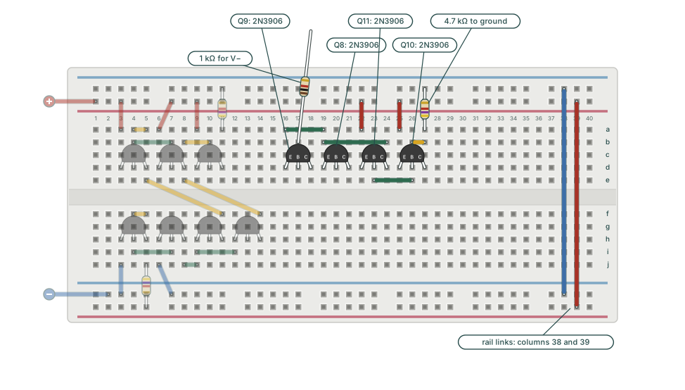
The breadboard drawn 40 columns wide, with the threshold comparator of Experiment 7 faded. Its two input resistors are gone from 10j and 13j. In colour: the rail links at columns 38 and 39, blue joining the two ground rails and red joining the two +5 volt rails. Four 2N3906 transistors stand in row d with their flat faces towards the near edge: Q9 at 16 to 18, Q8 at 19 to 21, Q11 at 22 to 24, Q10 at 25 to 27. Red jumpers connect 22a and 25a straight up to the inner top rail, +5 volts. A 4.7 kilohm resistor stands from 27a over the +5 volt rail to the outer top rail, ground. A green jumper joins 23e and 26e, a short yellow jumper joins 26b and 27b, a green jumper joins 19b and 24b, and a green jumper joins 16a and 19a. A 1 kilohm resistor stands in 17b, Q9's base column, and rises over the top rails, its free leg in the air.
Figure 8-3: The upper block of the trigger comparator: the PNP pair Q8 and Q9, the PNP tail mirror Q10 and Q11, and the 1 kΩ that will carry V− to Q9's base. Click to enlarge.

The steps follow Figure 8-3. Start with the power off.

  1. Switch everything off: the 5 V supply, power supply output 2 and the generator.
  2. Take the 1 kΩ resistors off the threshold comparator. Unclip the generator's red lead from the resistor in 10j and power supply output 2's positive lead from the resistor in 13j. Pull both resistors out. They belong to the leads, so they move to the new inputs with them.
  3. Move the rail links. Look for them in columns 28 and 29, where the drawings so far show them. Move the blue link to column 38 and the red link to column 39. The blue link joins the two ground rails, and the red link joins the two +5 V rails.
  4. Fit Q8 to Q11. Put four 2N3906 in row d, with their flat faces towards the near edge of the board. Q9 goes at 16d to 18d, Q8 at 19d to 21d, Q11 at 22d to 24d and Q10 at 25d to 27d. Each one's legs read emitter, base, collector from left to right.
  5. Connect the tail mirror's emitters to +5 V. Fit a jumper from 22a and one from 25a, each straight up to the top +5 V rail, the inner one.
  6. Connect Q10's base to its collector. Fit a short jumper from 26b to 27b.
  7. Join the two bases of the mirror. Fit a jumper from 23e to 26e.
  8. Fit the reference resistor. Fit a 4.7 kΩ resistor from 27a to the top ground rail, the outer one. It reaches over the +5 V rail. It sets the tail current, as the 4.7 kΩ on Q3 does in the threshold comparator.
  9. Connect the tail. Fit a jumper from 24b to 19b, from Q11's collector to Q8's emitter.
  10. Join the pair's emitters. Fit a jumper from 16a to 19a.
  11. Fit the 1 kΩ for V−. Push one leg of one of the two 1 kΩ resistors into 17b, in Q9's base column, and let it stand up over the top rails. Its free leg takes power supply output 2 once the circuit is complete.

The collectors of Q8 and Q9 are still unconnected. In the threshold comparator, the pair's collectors meet the PNP load. Here they meet the NPN load, in the lower block below the pair. Figure 8-4 adds the load, the output stage and the leads.
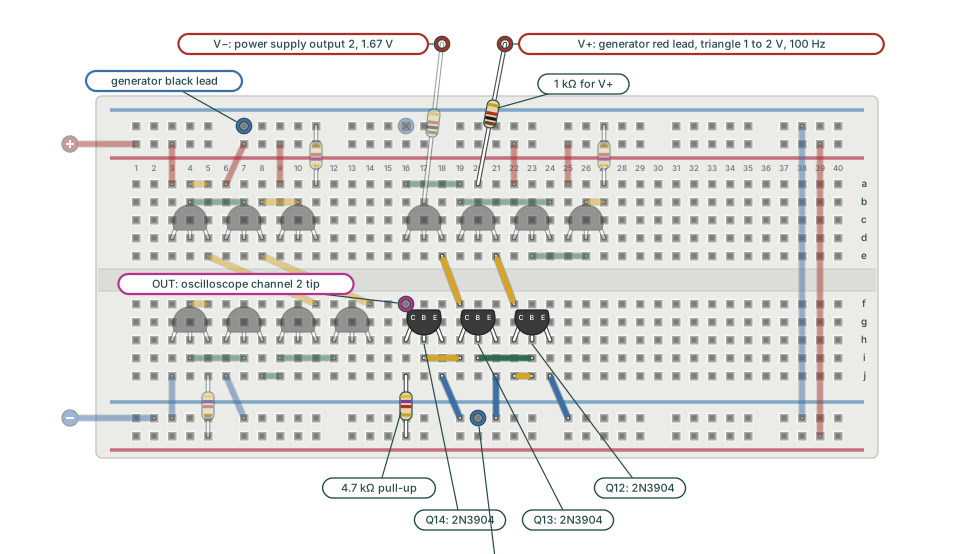
The breadboard with the threshold comparator and the upper block of the trigger comparator faded, the 1 kilohm resistor in 17b included. In colour: yellow jumpers from 18e to 19f and from 21e to 22f cross the centre channel on a diagonal. Three 2N3904 transistors stand in row h with their flat faces towards the far edge: Q14 at 16 to 18, Q13 at 19 to 21, Q12 at 22 to 24. A blue jumper connects 21j straight down to the inner bottom rail, ground, and two short blue jumpers run on a slant from 18j to the rail at column 19 and from 24j to the rail at column 25. A short yellow jumper joins 22j and 23j, a green jumper joins 20i and 23i, and a yellow jumper joins 17i and 19i. A 4.7 kilohm resistor stands from 16j over the ground rail to the outer bottom rail, +5 volts. A 1 kilohm resistor stands in 20a, Q8's base column, and rises over the top rails. Labels mark V+, the generator's red lead clipped onto that resistor's free leg, a triangle from 1 to 2 volts at 100 hertz, and V−, the positive lead of power supply output 2 clipped onto the free leg of the resistor in 17b, at 1.67 volts. They also mark the generator's black lead on the top ground rail at column 7, the oscilloscope channel 2 probe tip on OUT at 16f and its ground on the bottom ground rail at column 20.
Figure 8-4: The whole trigger comparator. The NPN load Q12 and Q13 stands under the pair, with Q14 beside it. The generator and the probe move across to the new circuit. Click to enlarge.
  1. Connect the collectors across the channel. Fit a jumper from 21e to 22f, for Q8's collector. Fit a jumper from 18e to 19f, for Q9's collector. Both jumpers cross the centre channel on a short diagonal.
  2. Fit Q12 to Q14. Put three 2N3904 in row h, with their flat faces towards the far edge. Q14 goes at 16h to 18h, Q13 at 19h to 21h and Q12 at 22h to 24h. Their legs read collector, base, emitter.
  3. Connect their emitters to ground. Fit a jumper from 21j straight down to the bottom ground rail, the inner one. The rail has no holes below columns 18 and 24, so fit a short jumper on a slant from 18j to the rail hole at column 19, and one from 24j to the rail hole at column 25.
  4. Connect Q12's base to its collector. Fit a short jumper from 23j to 22j.
  5. Join the two bases of the load. Fit a jumper from 20i to 23i.
  6. Connect node B to Q14's base. Fit a jumper from 19i to 17i. Column 19 of the lower block is Q13's collector. The jumper from 18e joins it to Q9's collector.
  7. Fit the pull-up. Fit a 4.7 kΩ resistor from 16j to the bottom +5 V rail, the outer one. It reaches over the ground rail. Column 16 of the lower block is Q14's collector: the trigger comparator's OUT.
  8. Fit the 1 kΩ for V+. Push one leg of the other 1 kΩ resistor into 20a, in Q8's base column, and let it stand up over the top rails. Clip the generator's red lead onto its free leg. Leave its black lead on the top ground rail.
  9. Connect V−. Clip the positive lead of power supply output 2 onto the free leg of the 1 kΩ in 17b. Set it to 1.67 V. Leave its negative lead on the top ground rail at column 16.
  10. Move the probe tip to 16f. Leave its ground clip on the bottom ground rail at column 20.

Each lead reaches its base through a 1 kΩ, for the reason Experiment 7 found: a base that conducts at the end of an instrument's lead can oscillate. The threshold comparator's inputs in 10j and 13j stay empty until the leads come back for the floor test.

The next section switches the power on. If OUT then stays near 0 V whatever the input does, Q14 is on all the time. Check that Q14 is a 2N3904 and that the pull-up goes to the outer bottom rail. If OUT stays at 5 V whatever the input does, check the jumpers from 18e to 19f and from 19i to 17i. Also check that Q8 to Q11 are 2N3906 with their flat faces towards the near edge. The 4.7 kΩ on Q10 must go to the outer top rail, ground: on the inner +5 V rail, the tail would carry no current.

Measure the output

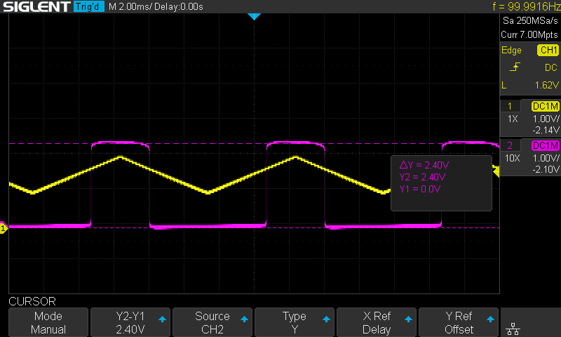
The new comparator is complete. The first check is the one that Experiment 7 made on the threshold comparator at 1.67 V: a triangle through the reference, and OUT on the oscilloscope. OUT should switch between 0 V and 5 V each time V+ crosses 1.67 V.
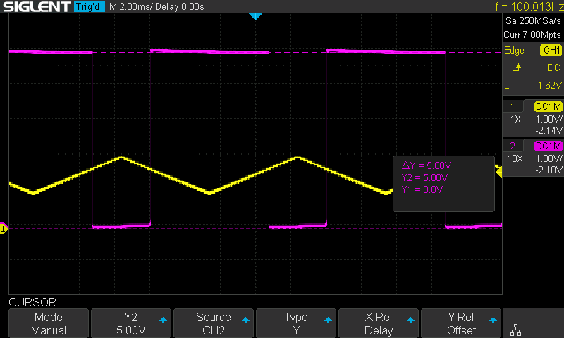
  1. Set the generator to a triangle from 1 V to 2 V at 100 Hz. Keep its load setting at HiZ.
  2. Set the oscilloscope as in Experiment 7: both channels at 1 V/div, the timebase at 2 ms/div. Trigger on channel 1, rising, at 1.62 V. Put the Y cursors on OUT's two levels.
  3. Switch on the 5 V supply, power supply output 2 and the generator.
Oscilloscope at 1 volt per division and 2 milliseconds per division, triggered on channel 1 rising at 1.62 volts, V− at 1.67 volts through the 1 kilohm resistor in 17b. The yellow input triangle, V+ through the 1 kilohm resistor in 20a, rises and falls between 1 and 2 volts. The magenta trace, the trigger comparator's OUT at 16f, sits near 5 volts while the input is below about 1.7 volts and near 0 volts while it is above. Both traces are thin. Y cursors read Y1 0.0 volts and Y2 5.00 volts.
Figure 8-5: V+ in yellow and the trigger comparator's OUT in magenta, with V− at 1.67 V. The cursors read 0.0 V and 5.00 V.

Figure 8-5 is the capture for this check. OUT switches between 0.0 V and 5.00 V each time V+ crosses about 1.7 V, near V−. It is high while V+ is below V−, the same way round as the threshold comparator's OUT. For the trigger, that is the useful sense. Its output goes high while the input is below 1/3 VCC, which is when the 555 has to start a new cycle.

What just happened?

The last section expects OUT at both rails. This section explains why, and what the reflected circuit does to the limits that Experiment 7 found at node A. Figure 8-6 marks the steps on the circuit. The tail is drawn as one current source hanging from +5 V.
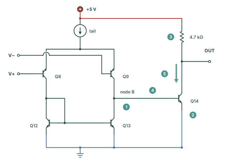
The trigger comparator with the tail drawn as a current-source symbol hanging from +5 volts above the joined emitters of the PNP pair Q8 and Q9. Below the pair is the NPN load Q12 and Q13 on ground. Node B, Q9's collector, runs to the base of Q14 at the right. Q14's emitter is on ground, and its collector is OUT, pulled up to +5 volts through 4.7 kilohms. Five numbered markers match the steps below. Marker 1: node B. Marker 2: Q14's emitter. Marker 3: the 4.7 kilohm pull-up. Marker 4: the wire from node B to Q14's base. Marker 5: a current arrow down Q14's collector.
Figure 8-6: The trigger comparator, with the five steps marked. The numbers match the list below.
  1. V+ below V−: node B falls. Q8's base is the lower of the two, so Q8 takes the tail current, about 0.93 mA. That current flows down through Q12, and Q13 copies it, pulling the same current out of node B. Q9 puts almost nothing in. So node B falls until Q13 saturates, a few hundredths of a volt above ground.
  2. Q14 is off. Its base, on node B, is within a few hundredths of a volt of its emitter on ground. An NPN needs about 0.65 V there to conduct.
  3. The pull-up holds OUT at +5 V. Q14 passes no current, so no current flows through the 4.7 kΩ, and OUT sits at the rail.
  4. V+ above V−: node B rises, and Q14 holds it near 0.65 V. Now Q9 takes the tail current and puts it into node B, and Q13 takes almost nothing out. Node B rises until it is about 0.65 V above ground. There Q14's base-emitter junction conducts, and Q9's current flows on into Q14's base. So node B stops rising near 0.65 V. Without Q14, node B would rise until Q9 saturated. A transistor lifts its collector only as far as its emitter. Q9's emitter sits one base-emitter drop above V−: about 1.67 + 0.65 = 2.3 V. That ceiling is Experiment 7's floor, reversed.
  5. Q14 pulls OUT down. With close to 1 mA in its base, Q14 could sink far more than that. The 4.7 kΩ lets only about 1 mA through before OUT reaches ground. So Q14 saturates, and OUT sits a few hundredths of a volt above 0 V.

Check node B

Step 4 makes two claims about node B. With Q14 connected, node B stops near 0.65 V. Without Q14, it would rise to about 2.3 V. You can check both by moving the probe to node B and removing one jumper.

With Q14 removed, nothing takes current from node B. So the whole tail current, up to 0.93 mA, leaves through Q9's base into V−. Through the 1 kΩ, that current would lift Q9's base by up to 0.93 V. For this check, power supply output 2 connects to Q9's base column directly, as in my first build, so V− stays at 1.67 V. Figure 8-7 shows the leads.
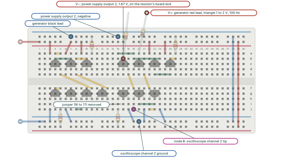
The breadboard with both comparators faded, the 1 kilohm input resistors in 17b and 20a included. The jumper from 19i to 17i is gone, and a pill points at its empty hole. Coloured rings and labels mark the leads. V− from power supply output 2, at 1.67 volts, hooks onto the lower leg of the 1 kilohm resistor where it enters 17b, and its negative lead is on the top ground rail at column 16. V+ from the generator's red lead reaches 20a through the 1 kilohm resistor standing there, a triangle from 1 to 2 volts at 100 hertz, and its black lead is on the top ground rail at column 7. The oscilloscope channel 2 probe tip is on node B at 19j, and its ground is on the bottom ground rail at column 20.
Figure 8-7: The node B check. Power supply output 2 reaches Q9's base without the 1 kΩ, and nothing joins node B to Q14. Click to enlarge.
  1. Switch off the 5 V supply, power supply output 2 and the generator.
  2. Remove the jumper from 19i to 17i. Nothing now connects node B to Q14.
  3. Move power supply output 2's positive lead from the free leg of the 1 kΩ in 17b to its lower leg, where it enters the board. The lead then reaches Q9's base without the resistor. Keep it at 1.67 V.
  4. Move the probe tip from 16f to 19j, in Q13's collector column.
  5. Switch on the 5 V supply, power supply output 2 and the generator. Put the Y cursors on node B's two levels.
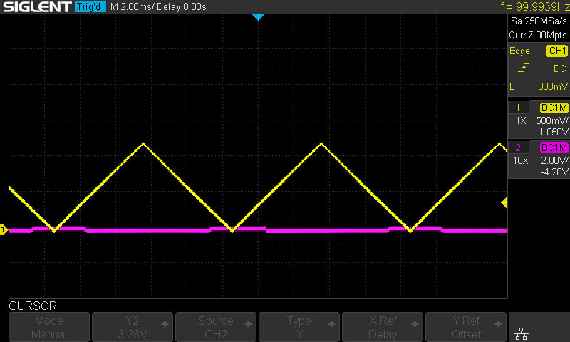
Oscilloscope at 1 volt per division and 2 milliseconds per division, triggered on channel 1 rising at 1.62 volts, V− at 1.67 volts from power supply output 2 connected straight to 17b, the jumper from 19i to 17i removed. The yellow input triangle rises and falls between 1 and 2 volts. The magenta trace, node B at 19j, sits at 0 volts while the input is below about 1.7 volts. While it is above, node B jumps up and stays level at about 2.4 volts, with slightly rounded corners. Y cursors read Y1 0.0 volts and Y2 2.40 volts.
Figure 8-8: Node B with nothing connected to it but the probe, and V− from power supply output 2. The cursors read 0.0 V and 2.40 V.

With V+ above V−, node B rises well above 0.65 V and stops at 2.40 V, far below +5 V. That is near V− + 0.65 V, about 2.3 V, but a little above it. My first build read 2.44 V here. The collector cannot rise past its emitter, so the emitter itself sits higher than the sum. With nothing taking current from node B, Q9's base carries the whole tail current. Its base-emitter drop is then more than the round 0.65 V: at least 2.40 V − 1.67 V = 0.73 V. Experiment 7's floor showed the same effect: 3.33 V − 2.64 V = 0.69 V.

If node B's high level climbs and falls with V+ instead of staying level, power supply output 2's lead is still on the free leg of the 1 kΩ. The tail current through the 1 kΩ then lifts Q9's base until Q8 starts to share the current. Q9's base follows V+, and node B follows it about 0.6 V higher. Move the lead to the resistor's lower leg, where it enters 17b.

Now reconnect Q14.
  1. Switch off the 5 V supply, power supply output 2 and the generator.
  2. Refit the jumper from 19i to 17i. Leave the probe at 19j.
  3. Move power supply output 2's positive lead back to the free leg of the 1 kΩ in 17b. With Q14 connected, Q9's base carries only microamps again.
  4. Switch on the 5 V supply, power supply output 2 and the generator. Move the Y cursors to node B's new levels.
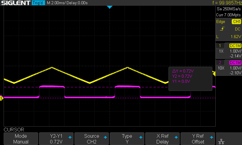
Oscilloscope at 1 volt per division and 2 milliseconds per division, triggered on channel 1 rising at 1.62 volts, V− at 1.67 volts from power supply output 2 through the 1 kilohm resistor in 17b, the jumper from 19i to 17i back in. The yellow input triangle rises and falls between 1 and 2 volts. The magenta trace, node B at 19j, sits at 0 volts while the input is below about 1.7 volts and steps up to a level of about 0.7 volts while it is above. Both traces are thin. Y cursors read Y1 0.0 volts and Y2 0.72 volts.
Figure 8-9: Node B with Q14's base on it. The cursors read 0.0 V and 0.72 V.

With Q14's base on it, node B's high level falls from 2.40 V to 0.72 V, Q14's base-emitter drop. My first build read about 0.9 V here. Q14 then turns that small swing into the full swing of OUT in Figure 8-5. Q7 did the same at node A in Experiment 7, where the low level sat 0.70 V below +5 V. The table lists the expected and measured levels, and the figures that capture them.

LevelExpectedMeasuredCaptureSet by
Node B high, Q14 disconnectedabout 2.3 V2.40 VFigure 8-8Q9's emitter, V− + 0.65 V
Node B high, Q14 connectedabout 0.65 V0.72 VFigure 8-9Q14's base-emitter junction
OUT high5 V5.00 VFigure 8-5the pull-up to +5 V

Why the trigger is PNP

The node B check explains how the twin reaches both rails. But Experiment 7 already ran the NPN threshold comparator with V− at 1.67 V, and its OUT read 0.0 V and 5.00 V there too. So on this board, at 1.67 V, the NPN comparator does the trigger's job as well. With V− at 1.67 V, the NPN pair's emitters sit near 1 V whatever V+ does. When V+ falls to 0 V, Q1 switches off.

The two pairs differ when both inputs are low. Figure 8-10 puts both inputs of each pair at 0.3 V. That is below 0.42 V, where the NPN comparator stopped switching in the floor test.
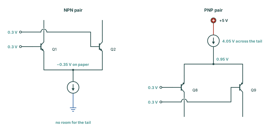
Two differential pairs side by side, with both inputs of each at 0.3 volts. Left, the NPN pair Q1 and Q2 with its emitters joined above a tail current source to ground. The emitter junction is tagged minus 0.35 volts on paper, and the tail is tagged no room for the tail. Right, the PNP pair Q8 and Q9 with its emitters joined below a tail current source hanging from +5 volts. The emitter junction is tagged 0.95 volts, and the tail is tagged 4.05 volts across the tail.
Figure 8-10: Both inputs of each pair at 0.3 V. On paper, the NPN pair's emitters would sit below ground, and its tail has no room. The PNP pair's emitters sit at 0.95 V, with 4.05 V left for its tail.

In the NPN pair, the emitters sit one base-emitter drop below the inputs. The tail mirror below them needs some voltage across it to keep its current. With the inputs at 0.3 V, the full 0.65 V drop puts the emitters at −0.35 V on paper, below ground. The emitters cannot go there, so the tail runs out of room and the pair runs out of current. The PNP pair has the same limit at the other end, near +5 V. Near ground, its emitters sit above the inputs, and its tail has most of the supply.

Where does the NPN pair stop? A first estimate adds one base-emitter drop, 0.65 V, to a couple of tenths for the tail mirror: about 0.9 V. The next section measures it.

Find the NPN pair's floor

The last section estimated the floor at about 0.9 V. The measurement uses the threshold comparator: its reference falls in steps while V+ keeps crossing it. Power supply output 2 moves back to the threshold comparator's V−, and the generator and the probe move with it. Figure 8-11 shows the leads.
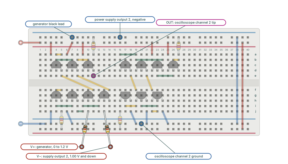
The breadboard with both comparators faded. In colour, the two 1 kilohm input resistors stand in 10j and 13j and lean out over the bottom rails, and 17b and 20a are empty. Coloured rings and labels mark the leads. V+, the generator's red lead, is back on the free leg of the 1 kilohm resistor in 10j, a triangle from 0 to 1.2 volts at 100 hertz. V−, the positive lead of power supply output 2, is on the free leg of the 1 kilohm resistor in 13j, stepped down from 1.00 volt. The generator's black lead and the negative lead of power supply output 2 are on the top ground rail at columns 7 and 16. The oscilloscope channel 2 probe tip is on the threshold comparator's OUT at 11e, and its ground is on the bottom ground rail at column 20.
Figure 8-11: The floor test. Power supply output 2, the generator and the probe are back on the threshold comparator, each input lead on its 1 kΩ in 10j or 13j. Click to enlarge.
  1. Switch off the 5 V supply, power supply output 2 and the generator.
  2. Move V−. Pull the 1 kΩ out of 17b, with power supply output 2's positive lead still clipped on its free leg. Push its other leg into 13j and let it lean out over the bottom rails. Set power supply output 2 to 1.00 V.
  3. Move V+. Move the 1 kΩ in 20a the same way, with the generator's red lead on it, into 10j. Set the generator to a triangle from 0 V to 1.2 V at 100 Hz.
  4. Move the probe tip from 19j to 11e, the threshold comparator's OUT.
  5. Set the oscilloscope to 500 mV/div on channel 1 and 2 V/div on channel 2, with the timebase at 2 ms/div. Trigger on channel 1, rising. Move each channel's ground marker near the bottom of the screen.
  6. Switch on the 5 V supply, power supply output 2 and the generator. OUT is high while the triangle is below V−.
  7. Step V− down: 1.00 V, 0.60 V, then 0.56 V. Continue down to 0.42 V in steps of a few hundredths of a volt. At each step, look at OUT's pulses.

At these voltages, the value you set on the supply and the voltage at its terminals can differ by a few tens of millivolts. That is the size of the steps. Read the measured output on the supply's display, or a multimeter from 13i to ground, and use that reading.
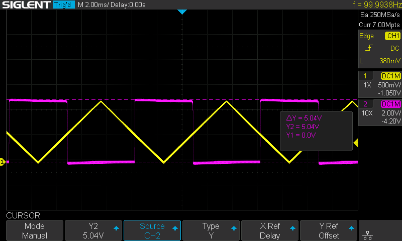
Oscilloscope at 2 milliseconds per division, channel 1 at 500 millivolts per division, channel 2 at 2 volts per division, triggered on channel 1 rising at 380 millivolts. V− is 0.56 volts from power supply output 2 through the 1 kilohm resistor in 13j. The yellow input triangle rises and falls between 0 and 1.2 volts. The magenta trace, the threshold comparator's OUT at 11e, is a train of full-height pulses with flat tops: it sits near 5 volts while the triangle is below about 0.6 volts and near 0 volts while it is above. Y cursors read Y1 0.0 volts and Y2 5.04 volts.
Figure 8-12: V− at 0.56 V. OUT still switches cleanly here, between 0.0 V and 5.04 V.
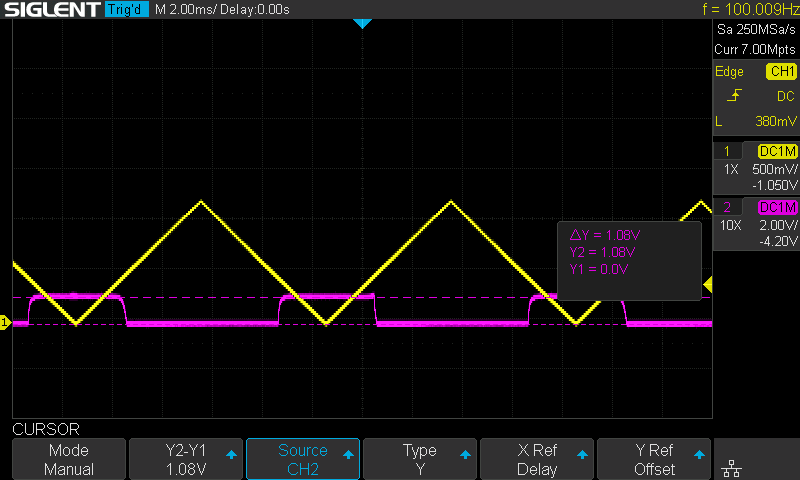
The same oscilloscope settings as Figure 8-12, with V− at 0.48 volts. The yellow input triangle rises and falls between 0 and 1.2 volts. The magenta trace, OUT, still switches where the triangle crosses about 0.5 volts, but its pulses are short: it rises only to about 1.1 volts while the triangle is below V−, with rounded corners, and sits near 0 volts the rest of the time. Y cursors read Y1 0.0 volts and Y2 1.08 volts.
Figure 8-13: V− at 0.48 V. OUT still switches, but its pulses reach only 1.08 V.
The same oscilloscope settings as Figure 8-12, with V− at 0.42 volts and the cursors off. The yellow input triangle rises and falls between 0 and 1.2 volts. The magenta trace, OUT, stays near 0 volts. It steps up by about a tenth of a volt while the triangle is below about 0.3 volts, a step that is barely visible at 2 volts per division.
Figure 8-14: V− at 0.42 V. OUT no longer switches. It rises by about 0.1 V while the triangle is near 0 V.

Figures 8-12 to 8-14 are three of the steps. The comparator switches cleanly well below the 0.9 V estimate. Then, over less than a tenth of a volt, OUT's pulses lose their height, and OUT stops switching. The table gives this board's readings beside those of my first build.

V−, measuredOUT on this boardOUT in my first build
0.56 Vfull-height pulses, 0.0 V to 5.04 V (Figure 8-12)full-height pulses with flat tops
0.50 Vnot measuredpulses, their tops starting to round
0.48 Vpulses only 1.08 V high (Figure 8-13)short, rounded pulses
0.45 Vnot measuredsmall bumps where V+ is lowest
0.42 Va step of about 0.1 V, no switching (Figure 8-14)flat, no switching

So the NPN pair's floor is near 0.45 V, about half the first estimate. On this board at 5 V, the trigger's 1.67 V reference sits more than a volt above that floor. So an NPN comparator would do the trigger's job here.

The NE555 has less margin, and that is probably why its trigger comparator is PNP. The chip puts two transistors on each input, a Darlington pair, which adds a second base-emitter drop. That would lift this floor to about 0.45 + 0.65 = 1.1 V. At the NE555's minimum supply of 4.5 V, the trigger's reference is 1.50 V, and the control pin can pull it lower still. A PNP pair keeps its tail's room at all of these levels.

Why the floor is lower than 0.9 V

The 0.9 V estimate assumes that the tail keeps its full current, about 0.93 mA, however low the inputs go. As V− falls, the emitters fall with it, and Q4, the tail's output transistor, has less and less voltage across it. When Q4 saturates, it passes less current. A smaller current needs a smaller base-emitter drop, about 60 mV less for each factor of ten. So the emitters can follow V− further down than the estimate allowed.

OUT keeps its full height while the tail still gives Q7's base the few microamps it needs. The pulses shrink when the tail current falls below that. That point works out near 0.55 V. On this board it lies between the 0.56 V reading, with full-height pulses, and the 0.48 V reading, where the pulses reach only 1.08 V. This explanation fits the readings. I have not measured the tail current near the floor.

Where the 0.55 V comes from optional

Q7 lifts OUT to +5 V through the 4.7 kΩ pull-down. The current that Q7 must pass is

If Q7's current gain is about 100, its base needs

While V+ is below V−, that base current is the tail current that Q2 takes out of node A. From the full tail current to 11 µA is a factor of

The number of factors of ten in 85 is its logarithm to base ten:

At about 60 mV for each factor of ten, the pair's base-emitter drop shrinks by

So the drop falls from about 0.65 V to

Q4 still needs a few hundredths of a volt across it, about 0.02 V. V− must sit at least this far above ground for the tail to pass 11 µA:

Below about 0.55 V, the tail passes less than Q7's base needs, and OUT's pulses lose height. In the table, the tops are flat at 0.56 V and start to round at 0.50 V.

The two polarities in the NE555

In Ken Shirriff's analysis of the NE555's die, the threshold comparator uses NPN transistors and the trigger comparator uses PNPs. In his words, this "allows the threshold comparator to work near the supply voltage and the trigger comparator to work near ground." The chip also puts a Darlington pair on each input, so its inputs sit two base-emitter drops from the pair's emitters. For an NPN pair, that would raise the floor measured here by another drop, to about 1.1 V.

The references

The floor test is complete. Leave the leads where they are: power supply output 2 and the generator on the threshold comparator's 1 kΩ resistors, and the probe on 11e, where Experiment 9 starts. Power supply output 2 has fed one comparator at a time. Experiment 9 replaces it with references made on the board, one for each comparator.

The flaw list

No flaw joins the list in this experiment. The trigger comparator is the threshold comparator turned over, and it keeps the fixes of Experiments 4 to 7. The NPN floor near 0.45 V is a question of margin in the NE555. On this board the trigger works with either pair at 1.67 V, so the floor stays off the list.

#FlawWhat it meansFoundStatus
1No reference inputThe threshold is the transistor's own 0.6 V. Nothing outside the circuit sets it.Experiment 3Fixed in Experiment 4: the differential pair
2Wide transitionThe output needs a band of input to travel from high to low: about half a volt with one transistor, about a quarter of a volt with the pair.Experiment 3Fixed in Experiment 6: the active load
3Thermal driftThe base-emitter voltage falls about 2 mV per degree, and the threshold falls with it.Experiment 3Reduced in Experiment 4: two matched transistors drifting together
4Tail current follows the common-mode levelA resistor tail passes more current as both inputs rise, and the output moves with it.Experiment 4Fixed in Experiment 5: the current mirror tail
5Output low trapped a diode drop below the referenceThe output's low level sits a diode drop below the reference instead of at ground.Experiment 6Fixed in Experiment 7: the PNP output stage

Quick check

Three questions on this experiment: node B's ceiling, what Q14 does to it, and why the trigger comparator uses PNPs.

1. With Q14 disconnected, node B cannot rise above about 2.3 V because…

Q9 saturates when its collector reaches its emitter. The pair holds its emitters one base-emitter drop above the lower input. With V− at 1.67 V, the ceiling is near 2.3 V: Experiment 7's floor at node A, reversed.

2. With Q14 connected and V+ above V−, node B stops near 0.65 V because…

When node B is about 0.65 V above ground, Q14's base takes Q9's current. Node B stays there, and Q14 switches on hard and pulls OUT to ground.

3. On this board the NPN threshold comparator switched cleanly with V− at 1.67 V. The NE555 still builds its trigger comparator from PNPs, probably because…

The floor test stopped this NPN comparator near 0.45 V. A Darlington input adds another drop, to about 1.1 V. At the NE555's 4.5 V minimum supply, the trigger's reference is 1.50 V, and the control pin can lower it further. A PNP pair holds its emitters above its inputs and hangs its tail from +5 V, so its limit is at the top of the supply.

Before moving on

The board now carries both of the 555's comparators. The threshold comparator has its NPN pair next to ground and takes 3.33 V. The trigger comparator, the same circuit turned over, has its PNP pair next to +5 V and takes 1.67 V. The threshold comparator's output switches between 0 V and 5 V, and the trigger comparator's output should do the same. Both outputs are high while V+ is below V−.

The floor test measured how close to ground the NPN pair keeps working: near 0.45 V, on this board and in my first build. The NE555's Darlington inputs and lower supplies leave less room than that, which is probably why its trigger gets the PNP pair.

Both references still come from power supply output 2, one comparator at a time. Experiment 9: The Voltage Divider makes them on the board from the 5 V rail and measures how they follow the supply. It also shows why that removes the supply from the 555's timing.

Contents All experiments