Full Stack Electronics · Stage Four · Experiment 17
The fourth step from the breadboard to a printed circuit board. Choose a package for each part, give each symbol in KiCad its footprint, and check that no symbol is without one.
Experiment 16 showed that the KiCad schematic runs as a timer. The schematic still has no sizes. A symbol has pins, but no pads and no area on a board. The PCB Editor of Experiment 18 needs a footprint for each symbol: the pattern of copper pads that the part is soldered on. The footprint also sets how much of the board each part takes. The breadboard used through-hole parts, with leads that go through holes: transistors in the TO-92 package and resistors with wire leads. Their footprints take about three times the area of the surface-mount parts of the board. This experiment chooses surface-mount packages that you can solder by hand: SOT-23 transistors and 0805 resistors. Then it gives each of the 51 symbols its footprint and checks the result in a bill of materials.
The lead used two words for the same part: package and footprint. The package is the body of the part, which you buy. SOT-23 is a standard package for small transistors, and 0805 is a standard size of resistor and capacitor. The footprint is the drawing of copper for one package, in KiCad's library. Experiment 15 showed how the two connect: KiCad puts pin 1 of the symbol on pad 1 of the footprint. That is why the board uses the MMBT3904 and MMBT3906 symbols, which number their pins as the SOT-23 package does.
The name of a KiCad footprint says what it is. The table reads the name of the resistor footprint of this board, Resistor_SMD:R_0805_2012Metric_Pad1.20x1.40mm_HandSolder, part by part.
| Part of the name | Meaning |
|---|---|
Resistor_SMD | The library: resistors for surface mounting. SMD means surface-mount device. The colon ends the name of the library. |
R | A resistor |
0805 | The size code in inches: 0.08 by 0.05 inch |
2012Metric | The same size code in millimetres: 2.0 by 1.2 mm |
Pad1.20x1.40mm | Each pad is 1.20 mm by 1.40 mm |
HandSolder | The pads are longer than the standard pads, for soldering with an iron |
Resistors and capacitors come in a series of sizes. The table gives four of them, with the body of the part as KiCad's footprints draw it.
| Size code, inches | Size code, millimetres | Body |
|---|---|---|
| 1206 | 3216 | 3.2 × 1.6 mm |
| 0805 | 2012 | 2.0 × 1.25 mm |
| 0603 | 1608 | 1.6 × 0.82 mm |
| 0402 | 1005 | 1.05 × 0.54 mm |
This board uses 0805. Experiment 20 solders each part by hand with an iron and tweezers. An 0805 is large enough to hold, see and turn on the board. A 1206 is easier to hold, but its hand-solder footprint takes 11 mm² against 7 mm² for the 0805.
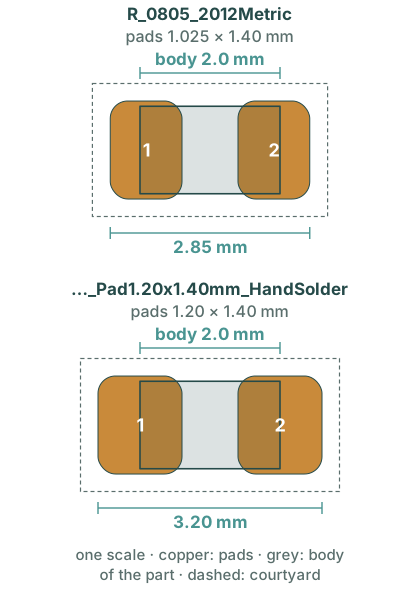
Figure 17-1 shows the difference between the two 0805 footprints of the KiCad library. The body of the part is the same in both. The hand-solder pads are 1.20 mm long in place of 1.025 mm, so each pad reaches 0.175 mm further past the end of the part. The tip of the iron touches that copper, and the solder flows up the end of the part from there.
The packages of the board are not those of the breadboard. Each footprint has a courtyard, the area around the part that no other part may enter. Figure 17-2 shows the through-hole footprints of the breadboard parts and the surface-mount footprints of the board, to one scale.
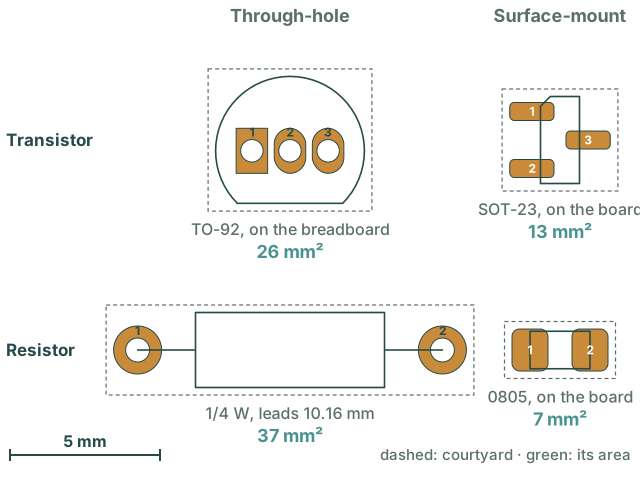
The board has 23 transistors and 21 resistors. In TO-92 and through-hole footprints, their courtyards take 1368 mm². In SOT-23 and 0805, they take 449 mm², about one third. The board is 46 mm by 56 mm, which is 2576 mm². So the through-hole courtyards alone would take 53 % of the board, before one track. A surface-mount part also needs no holes. It uses the copper on one side of the board only.
Those are the reasons for the packages. The table gives the footprint for each symbol of the board. The column on the right shows which symbols arrive with a footprint from the KiCad library.
| Parts | Package | KiCad footprint | From the symbol |
|---|---|---|---|
| Q1 to Q23, 16 NPN and 7 PNP | SOT-23 | Package_TO_SOT_SMD: | Yes |
| R1 to R21 | 0805 | Resistor_SMD: | No |
| C1 | 0805 | Capacitor_SMD: | No |
| J1 | Pin header, through-hole | Connector_PinHeader_2.54mm: | No |
| TP1 to TP5 | No part, a copper pad | TestPoint: | No |
The MMBT3904 and MMBT3906 symbols have SOT-23 as their default footprint, so the transistors got it in Experiment 15. The symbols R and C of the library Device are for any size of part, so they have no default. The same applies to the header and the test pad. That leaves 28 symbols to assign.
J1 is the only through-hole part. Its pins are the eight pins of the chip. They are standard header pins, which fit the sockets of the jumper leads to the breadboard. Each pad is 1.7 mm across with a 1.0 mm hole for a pin. The footprint puts the eight pads in one row, 2.54 mm apart. On the board of this course they stand four on each side, in the pin order of the NE555, and Experiment 18 places them. A test pad is a copper circle 1.0 mm across, with nothing soldered on it, for a probe.
The board carries the 555 only. RA, RB, the timing capacitor and the LED stay on the breadboard, as the test bench of Experiment 16 did. C1 is the one capacitor on the board, across the supply.
The table gives the footprint for each symbol. KiCad has a tool that shows all the symbols and the footprint libraries in one window, the Footprint Assignment Tool. Use the master project. The copy 555-sim does not go to the board.
555 and its Schematic Editor. Select Tools → Assign Footprints…. The left pane lists the footprint libraries, the middle pane lists the symbols, and the right pane lists footprints.Package_TO_SOT_SMD:SOT-23. If you started from the ZIP of Experiment 15, all 51 symbols already have their footprints. Then check each line against the table and continue at step 6.Resistor_SMD. In the right pane, double-click R_0805_2012Metric_Pad1.20x1.40mm_HandSolder. The tool gives R1 the footprint and selects the next symbol without one. Double-click the same footprint again for each resistor, to R21.Capacitor_SMD, and double-click C_0805_2012Metric_Pad1.18x1.45mm_HandSolder. Select J1, then the library Connector_PinHeader_2.54mm, and double-click PinHeader_1x08_P2.54mm_Vertical.TestPoint, and double-click TestPoint_Pad_D1.0mm once for each of TP1 to TP5.The filter buttons of the toolbar make the list of footprints shorter. One shows only the footprints that the filters of the symbol allow. Another shows only the footprints with the same number of pads as the symbol has pins. The KiCad library symbols have filters for this use. With both on, the list for R1 holds only resistor footprints with two pads.
The assignments are now in the schematic, and a bill of materials lists them. ERC does not report a symbol without a footprint. It reports a footprint name that is not in the library, for example “Footprint 'R_0805_Wrong' not found in library 'Resistor_SMD'”. A missing footprint shows only in the bill of materials.
"R1","4K7","","1" in the CSV file. Assign a footprint to it and look again.The courtyard of Figure 17-2 is in each footprint file, on a layer of its own. The design rules checker of the PCB Editor, in Experiment 19, reports footprints whose courtyards overlap. The body outline is on a further layer, for drawings of the assembly. Each footprint also names a 3D model of the part, so the 3D viewer of step 6 can show the part on its pads.
Three questions on this experiment. They ask what a footprint name says, why the pads are longer, and what finds a missing footprint.
1. In R_0805_2012Metric, what is 2012Metric?
0805 is the size in hundredths of an inch, 0.08 by 0.05. 2012 is the same size in tenths of a millimetre, 2.0 by 1.2. Neither says the value of the resistor.
2. Why does the board use the HandSolder footprints?
The body is the same in both footprints. The hand-solder pads are 1.20 mm long in place of 1.025 mm, so each pad shows 0.175 mm more copper past the end of the part.
3. R7 has no footprint. What shows it?
ERC checks connections and footprint names that are not in the library. It does not report an empty Footprint field. The simulation does not use footprints. The bill of materials groups the symbols by value and footprint, so R7 gets a line of its own.
Each of the 51 symbols has a footprint. The 23 transistors have SOT-23, the 21 resistors and C1 have 0805 with hand-solder pads, J1 has the 1×8 header, and each test pad has a 1.0 mm pad. The bill of materials has the 13 lines of the CSV in the box “Resources”. That is the fourth step from the breadboard to the board. The footprints have sizes, but no positions yet. Experiment 18: The Board places them on a board outline and draws the copper between them.