Full Stack Electronics · Stage Four · Experiment 18
The fifth step from the breadboard to a printed circuit board. Draw the outline, place the 51 footprints as seven blocks, route the tracks and pour the ground, until the design rules checker finds nothing to report.
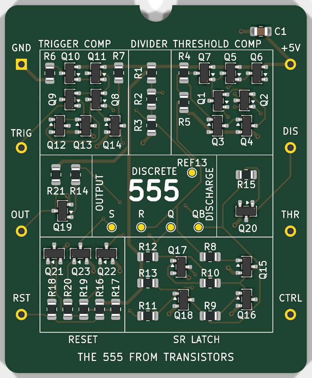
Experiment 17 gave each of the 51 symbols a footprint. The footprints have sizes, but no positions, and no copper connects them. The layout gives the board an outline, puts each footprint at its place, and draws copper for each connection of the netlist. The schematic cannot show the things that the layout decides: which parts sit side by side, how long each connection is, and where the ground current flows back. This experiment makes the layout of the board of this course in KiCad's PCB Editor. The board has the shape of an NE555, with the eight pins of the chip at its edges. So it can take the place of the chip on the breadboard of Experiment 1. The result is the board of Figure 18-1, and a check by the design rules checker that reports zero errors and zero connections that are not routed.
555.kicad_pcb and the six sheets. Open it to compare with your layout, or to start Experiment 19 without a layout of your own.
Figure 18-1 is the end of this experiment. The start is a board file with no outline and no footprints. The PCB Editor gets the footprints and the netlist from the schematic.
555.kicad_pcb. If the file does not exist yet, KiCad makes it.The ratsnest shows what to connect. Before the parts can go anywhere, the board needs its outline. This board has the shape of the chip that it replaces. Its pins are J1, at the edges, in the order of the NE555: pin 1 at the top left next to the notch, then anticlockwise, as Experiment 1 counted them. Eight jumper leads connect each pin to the row of the breadboard where the same pin of the NE555 sat. The rest of the circuit of Experiment 1 stays as it is.
The netlist connects each net to a pad number, so the new positions of the pads change nothing in the schematic. Pad 1 is square, so the board shows pin 1 as a chip does.
With the outline in place, set the rules for the copper before you route. KiCad uses these rules while you draw tracks, and the design rules checker tests the board against them. Select File → Board Setup…. The table gives the values of this board. None of them asks more than the usual process of a board factory.
| Section of Board Setup | Setting | Value |
|---|---|---|
| Physical Stackup | Copper layers, board thickness | 2, 1.6 mm |
| Constraints | Minimum clearance | 0.2 mm |
| Constraints | Minimum track width | 0.2 mm |
| Constraints | Copper to board edge clearance | 0.3 mm |
| Constraints | Minimum text height and thickness | 1.0 mm, 0.15 mm |
| Net Classes | Default: track, via, via hole | 0.254, 0.610, 0.305 mm |
| Net Classes | Power: track, via, via hole | 0.508, 0.813, 0.406 mm |
A net class is a set of nets with the same track width and via size. In the lower part of the section Net Classes, assign the patterns +5V and GND to the class Power. Then KiCad draws each supply track 0.508 mm wide and each signal track 0.254 mm wide, with no further setting. The values are 10 and 20 thousandths of an inch. If a field shows an odd value such as 3.937, its unit is a thousandth of an inch: 3.937 is 0.1 mm. Type the unit with the value, as in 0.2mm, and KiCad converts it.
The rules are set, and the 51 footprints are still a group beside the outline. Do not place them one by one. The board is the seven blocks that Stage Three built: the two comparators, the divider, the latch, the output stage, the discharge transistor and the reset block. Most of the connections stay inside one block. Figure 18-2 shows where each block sits on this board.
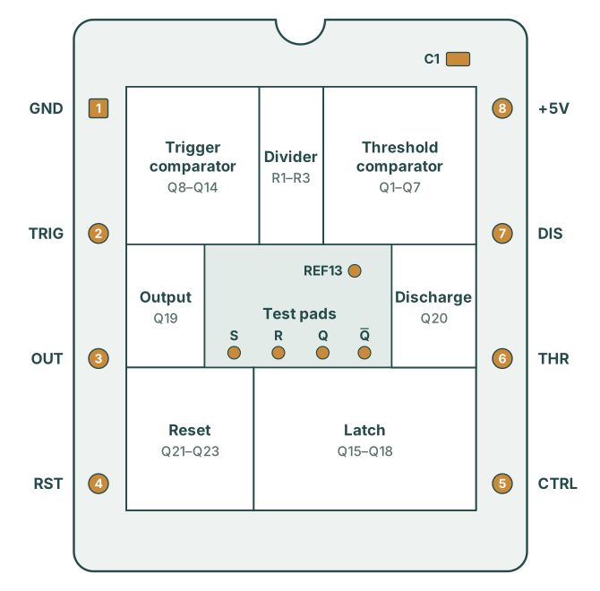
Only six signal nets join two blocks or more. The table gives them, with the blocks that each one joins. Apart from +5 V and GND, five of them have the longest tracks of the board, from 76 mm for Q̄ to 38 mm for Q. REF13 has 21 mm, because the divider sits next to the trigger comparator. So the blocks that share a net sit next to each other where they can.
| Net | From | To |
|---|---|---|
| CONTROL | Divider, the 2/3 tap | Threshold comparator, and pin 5 |
| REF13 | Divider, the 1/3 tap | Trigger comparator |
| R | Threshold comparator | Latch |
| S | Trigger comparator | Latch, and Q23 of the reset block |
| Q | Latch | Q22 of the reset block |
| Q̄ | Latch | Output, through R14, and discharge, through R15 |
The two comparators take an input from the divider, so the three sit side by side at the top. The latch sits under them, at the bottom right, and the reset block beside it, because Q and S run between the two. The output and discharge transistors sit in the middle row, next to their pins: Q19 near OUT on the left, Q20 near DIS on the right. C1 sits beside pin 8, where +5 V comes onto the board.
With each part in its place, the ratsnest is short, and each line becomes a track. Route inside each block first, then the six nets between the blocks, then the pins.
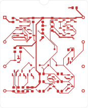
Figure 18-3 has no ground track. The ground is one sheet of copper on the back of the board, a zone. Each ground pad on the front connects to it through a via next to the pad. A sheet gives each ground connection a short and wide path to each other one. On a breadboard, the ground return went through the rails and the jumper wires.
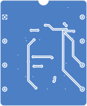
The zone is full, and the board has all its copper. The design rules checker now tests the copper against the rules of Board Setup and against the schematic.
The first full check of this board, after I routed it by hand, did not give zero. The tab Unconnected Items was empty, but the tab Violations had three errors. A track of RST, the collector net of Q21, landed on the wrong pad of R20 and shorted the resistor, so Q23 would have had no base resistor. Two ground vias were too close to the collector pads of transistors. One short track ended on nothing. A zone that I had not filled again after the last tracks also gave 58 clearance violations, and those went with B. The short across R20 is the important one. The timer would run with it, because the timer does not use the reset, so the fault would show only at the first reset of the board.
After the corrections, the board of this course gives 0 violations, 0 unconnected items and 0 parity issues. Its Board Setup sets some checks to ignore. With those checks on, the checker gives one warning: “Footprint 'PinHeader_1x08_P2.54mm_Vertical' does not match copy in library 'Connector_PinHeader_2.54mm'”, on J1. That is correct, because the pads of J1 moved. If your checker gives this warning, right-click it and select Exclude with comment…, with a comment such as “pads moved to the edges”. Then the checker shows the exclusion with its reason, and it continues to compare the footprints of all the other parts with the library.
The checker compares the board with rules and with the schematic. It does not know whether the pins are in the right order for the breadboard, or whether a probe can reach the test pads. It also does not know whether the files for the factory show the board that you drew. Experiment 19 checks those things before the order.
Three questions on this experiment. They ask what the ratsnest is, why the parts go in blocks, and what the ground zone does.
1. After F8, thin lines join the pads. What are they?
The ratsnest shows the connections that are still to make. Each track that reaches its pad removes one line. The tab Unconnected Items of the design rules checker lists the lines that are left.
2. Why place the parts as seven blocks?
The seven blocks are the circuits of Stage Three. With each block in one area, its connections are short, and only CONTROL, REF13, R, S, Q and Q̄ cross from one block to another.
3. What does the GND zone on the back give the board?
The zone is one sheet of copper on the net GND. Each ground pad on the front connects to it through a via, so no ground connection needs a track across the board.
The board has its outline, its 51 footprints in seven blocks, 269 track segments, 31 vias and a ground zone on the back. The design rules checker reports 0 violations, 0 unconnected items and 0 parity issues, apart from the expected warning for J1. That is the fifth step from the breadboard to the board. Experiment 19: Before You Order checks the board in the ways that the checker cannot, writes the files for the factory and orders the board.