Full Stack Electronics · Stage Four · Experiment 15
The second step from the breadboard to a printed circuit board. Enter the master schematic in KiCad, sheet by sheet, and check it with the electrical rules checker until it reports no errors.
Experiment 14 drew the master schematic on paper: five sheets, the named nets and a list of the parts. A factory cannot make a board from paper. It needs files that give the exact position of each copper pad, track and hole. KiCad is a free program that goes from a schematic to those files. You draw the circuit in KiCad, and KiCad checks its connections. Then you place the parts on a board outline and draw the copper between them, and KiCad writes the files for the factory. The link between the two halves is the netlist: a list of each net and the pins on it, which KiCad makes from the schematic. The board editor reads the netlist and shows which pads to connect, so each track on the board comes from a wire in the schematic. So the schematic comes first. This experiment enters the master schematic in KiCad and checks it with the electrical rules checker, ERC. The result is a KiCad schematic that has zero ERC errors and the same nets as the net table of Experiment 14.
KiCad is free and open source, and it runs on Windows, macOS and Linux. This course uses version 10. Each step of Stage Four from here to the order uses a part of KiCad. The table gives them.
| Step | Part of KiCad | Experiment |
|---|---|---|
| Enter the schematic and check its connections | Schematic Editor and its electrical rules checker (ERC) | 15 |
| Simulate the circuit before any part exists | Simulator, in the Schematic Editor | 16 |
| Give each part a footprint | Footprint assignment, in the Schematic Editor | 17 |
| Place the parts and draw the copper | PCB Editor | 18 |
| Check the board and write the files for the factory | Design rules checker (DRC) and Gerber plot, in the PCB Editor | 19 |
A KiCad project is a folder of text files with one name: the project file 555.kicad_pro, one .kicad_sch file for each sheet of the schematic, and the board file 555.kicad_pcb. Because the files are text, git can keep the history of a design, as it does for code. The first window is the Project Manager, which opens each editor. This experiment uses the Schematic Editor only.
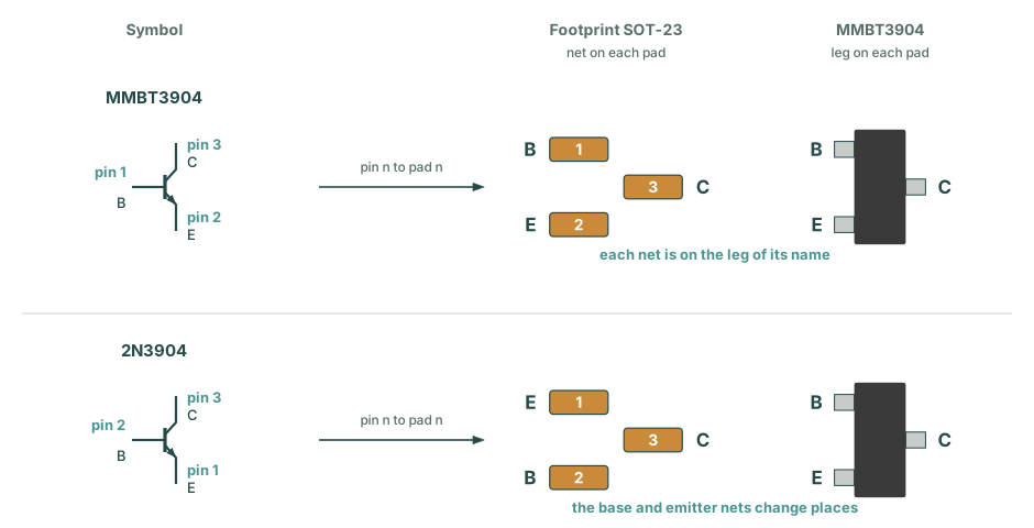
The Schematic Editor draws each part as a symbol. A symbol has pins, and each pin has a number, a name and an electrical type. The board uses a footprint for each part: the copper pads that the part is soldered on. Each pad has a number too. KiCad connects pin 1 of the symbol to pad 1 of the footprint, pin 2 to pad 2, and so on. The names B, C and E have no effect on that connection. Figure 15-1 shows why this matters.
The board uses the MMBT3904 and MMBT3906, the 2N3904 and 2N3906 in the SOT-23 package. Use the symbols with those names, in the library Transistor_BJT. They number the pins 1 B, 2 E, 3 C, as the SOT-23 package, and they already name the SOT-23 footprint. The symbols 2N3904 and 2N3906 number the pins 1 E, 2 B, 3 C, for the TO-92 package. The symbols Q_NPN and Q_PNP in the library Device use the letters B, C and E as pin numbers. No footprint has pads with those names.
ERC does not compare a symbol with a footprint. With the 2N3904 symbol, the schematic passes ERC, and each transistor on the board has its base and emitter changed. So choose the symbol by its name before you place the first transistor.
The MMBT symbols are the first rule for the capture. Before the 555 with its twenty-three transistors, practise the Schematic Editor and ERC on a circuit that you know. Figure 15-2 is the transistor switch of Experiment 3 with KiCad's designators. J1 is a three-pin header for +5 V, IN and ground. J2 is a one-pin header for OUT. On the 555 board, J1 is the eight pins.
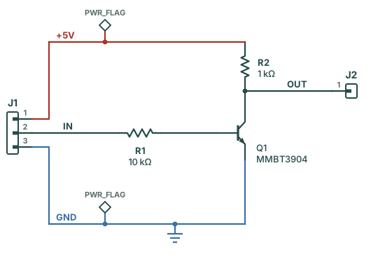
switch. Double-click switch.kicad_sch to open the Schematic Editor.MMBT3904, select it and click on the sheet to place it. In the same way, place two R from the library Device, one Conn_01x03_Pin and one Conn_01x01_Pin from the library Connector. Press R to turn a part while you place it, and X to turn J2 round so that its pin points left.10k for R1 and 1k for R2.+5V symbol on the wire from J1 pin 1 and a GND symbol on the wire from J1 pin 3. A power symbol gives its net a name. Each +5V symbol on any sheet is on the same net.+5V symbol and one on the GND symbol. Press P again and place a PWR_FLAG on the +5V wire and one on the GND wire. Run ERC again. It reports no errors and no warnings.Each pin of a symbol has an electrical type, such as input, output, passive or power input. ERC checks the pins on each net against a table of the types that can connect. The pin of a +5V or GND symbol is a power input, so ERC looks for a power output on the same net. On this circuit the supply comes from the bench power supply through J1, and J1's pins are passive. A PWR_FLAG has one power output pin. It tells ERC that the net gets power from outside the schematic. ERC is similar to a linter: it checks rules of connection. It cannot tell if the circuit does what it must do.
The practice circuit fits on one sheet. The KiCad project of the 555 has a root sheet and five sheets under it. Experiment 14 drew the master schematic in the same way, as a top sheet and block sheets. Figure 15-3 shows how one sheet connects to the root sheet.
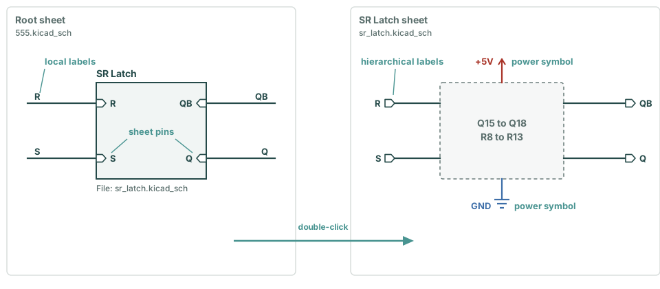
sr_latch.kicad_sch. Each sheet pin on the box connects to the hierarchical label with the same name inside that sheet.KiCad has four ways to connect by name. The 555 project uses the first three.
| Object | Key | What it connects |
|---|---|---|
| Hierarchical label | H | A net inside a sheet to the sheet pin with the same name on the sheet symbol |
| Local label | L | All wires with the same name on one sheet. The root sheet uses them for the test pads and J1. |
| Power symbol | P | All +5V on all sheets, and all GND. So no sheet has a sheet pin for the supply. |
| Global label | Ctrl+L (⌘+L on a Mac) | All wires with the same name on all sheets. The project does not use them. |
The table gives each sheet of the project. The parts and their designators are the same as in Experiment 14. The sheet UI holds J1, the eight pins of the board, and the two PWR_FLAG symbols. On the top sheet of your print, J1 is the eight pin badges on the board outline.
| Sheet, file and page of the print | Parts | Hierarchical labels |
|---|---|---|
(root)555.Page 1 | R1–R3, Q19, Q20, R14, R15, R21, C1, TP1–TP5 | None |
Threshold Comparatorthreshold_Page 2 | Q1–Q7, R4, R5 | THRESHOLD, REF23, R |
Trigger Comparatortrigger_Page 3 | Q8–Q14, R6, R7 | TRIGGER, REF13, S |
SR Latchsr_Page 4 | Q15–Q18, R8–R13 | R, S, Q, QB |
Resetreset.Page 5 | Q21–Q23, R16–R20 | RESET, Q, S |
UIui.Page 1 | J1, two PWR_FLAG | TRIGGER, OUTPUT, RESET, CONTROL, THRESHOLD, DISCHARGE |
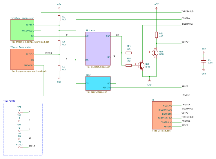
Two names differ from the print. The project writes Q̄ as QB. In the threshold comparator, the input from the 2/3 tap is the hierarchical label REF23. On the root sheet, a wire connects its sheet pin to the 2/3 tap, which has the local label CONTROL. A local label has priority over a hierarchical label, so the net name is CONTROL, as in the net table.
With the four kinds of connection, you can enter the whole schematic. Do one sheet at a time, and run ERC after each sheet. One sheet has few errors to find. Twenty-three transistors at once can have many.
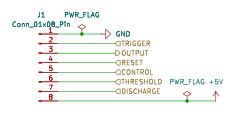
555. Open 555.kicad_sch, the root sheet.MMBT3904 for each NPN and MMBT3906 for each PNP. Give each part the designator and value of page 2 of your print with U and V. For 4.7 kΩ, type 4.7k or 4K7. Draw the wires with W. Add +5V and GND with P. The positions on your sheet can be different from the print. The connections must be the same. Figure 15-5 shows this sheet in the KiCad project.THRESHOLD and THRESHOLD_ are two different nets.Conn_01x08_Pin. Put a hierarchical label on pins 2 to 7, +5V on pin 8 and GND on pin 1. Put a PWR_FLAG on the wire of pin 8 and on the wire of pin 1. Figure 15-9 shows this sheet.C from Device. Connect the sheet pins with wires. Where a wire is long, use a local label with L at each end. Place TP1 to TP5 (TestPoint from Connector) and put a local label on each with its net name.Figure 15-4 is the root sheet of the KiCad project that the boards were made from. Your root sheet can have a different arrangement. Its connections must be the same.
Figures 15-5 to 15-9 are the five sheets under the root, in the order of the table after Figure 15-3. Each sheet has its own +5V and GND symbols, and a hierarchical label on each wire that leaves the sheet. Compare each figure with its page of your print. The connections are the same. The arrangement on the sheet is different in some places: for example, REF23 comes in from the right on the threshold sheet.
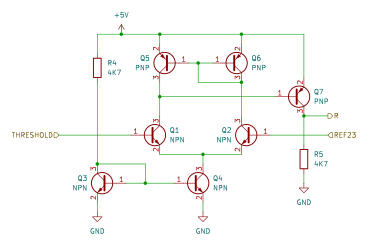
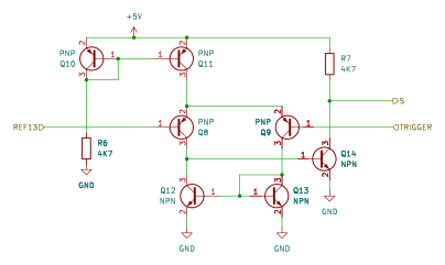
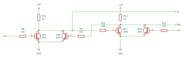
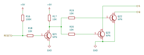
The steps end when ERC is clean. These are the messages that a capture of this schematic usually gives, from KiCad 10.
| Message | Usual cause | Correction |
|---|---|---|
| Input Power pin not driven by any Output Power pins | No PWR_FLAG on +5V or GND | A PWR_FLAG on each supply wire of the UI sheet |
| Pin not connected | A wire end stops near a pin and does not touch it, or a sheet pin has no wire | Draw the wire again, from pin end to pin end |
| Sheet pin QB has no matching hierarchical label inside the sheet, with Hierarchical label Q_B has no matching sheet pin in the parent sheet | The label inside the sheet has a different spelling from the sheet pin | Type the same name on the label and on the pin |
| Label connected to only one pin | A local label has a different spelling from its partner, so it makes a net of its own | Correct the spelling |
| Input pin not driven by any Output pins | A base is on a net with no other pin, as the bases of Q1 and Q2 before the root sheet connects THRESHOLD and CONTROL | Connect the net. Then the error goes. |
ERC checks the rules of connection only. The 2N3904 symbol of Figure 15-1, a wrong value such as 10K for R4, and a wire to the wrong pin all pass ERC. Two wires that cross also pass, and they are not connected. KiCad connects two wires that cross only where it shows a junction dot. The comparison of the nets in step 10 finds these errors, because it compares your schematic with the design.
Three questions on this experiment. They ask what ERC can find, how a sheet connects, and why the PWR_FLAG is there.
1. You place the 2N3904 symbol for each NPN and give it the SOT-23 footprint. ERC…
KiCad connects pin n to pad n. The 2N3904 symbol has E on pin 1 and B on pin 2. The MMBT3904 has its base on pad 1 and its emitter on pad 2. ERC does not compare symbols with footprints, so it cannot find this.
2. Inside sr_latch.kicad_sch a hierarchical label is Q_B. On the root sheet the sheet pin is QB. ERC…
A sheet pin connects only to the hierarchical label with the same name. With two names, there are two nets, and ERC gives an error on each side.
3. Why does the UI sheet have two PWR_FLAG symbols?
The pins of the +5V and GND symbols are power inputs. ERC looks for a power output on each of the two nets. The bench supply is outside the schematic, so a PWR_FLAG on each net tells ERC that the net gets power.
The master schematic is now a KiCad schematic. It has six sheets, ERC reports zero errors, and its nets are the nets of Experiment 14. That is the second step from the breadboard to the board. ERC shows that the connections obey the rules. It does not show that the circuit runs as a timer. Experiment 16: The Smoke Test simulates this schematic in SPICE, before you buy any part.