Full Stack Electronics · Stage Four · Experiment 14
The first step from the breadboard to a printed circuit board. Draw the whole 555 as one master schematic, give each part and each connection a name, list the parts, and record where the board differs from the breadboard.
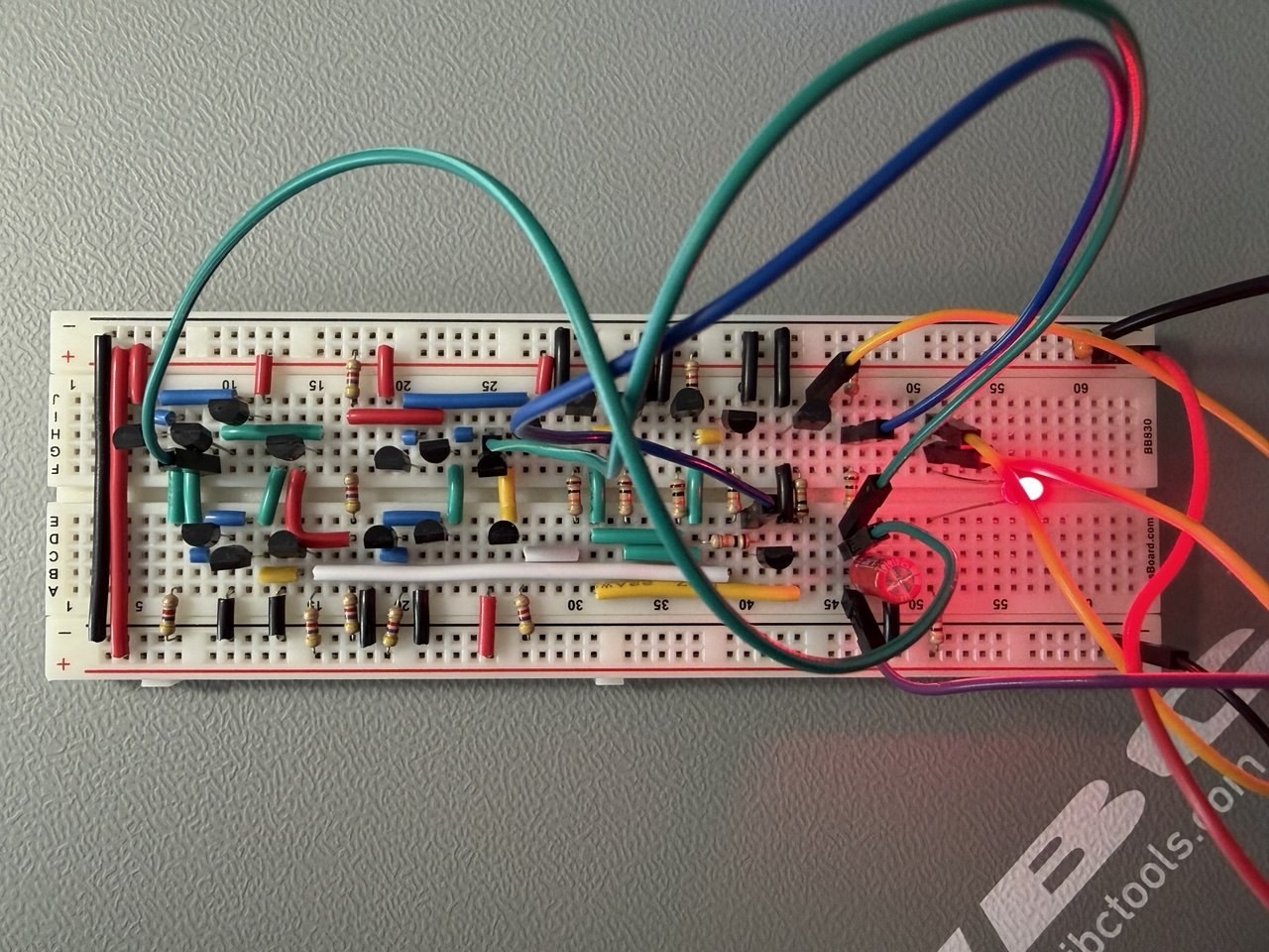
Experiment 13 completed Stage Three, and with it the first milestone of the course: a 555 from twenty-three transistors on a breadboard. It ran at 192.59 ms in Experiment 12, near the 200.46 ms of the NE555 chip in Experiment 1, and RESET stops it as it stops the chip. But the prototype fills most of a full-size breadboard, and one loose jumper can stop it. Stage Four makes the same circuit into a small printed circuit board, which connects to the breadboard of Experiment 1 through the eight pins of the chip that it replaces. The second milestone is a board design that is ready to order, and this experiment is the first step to it. It draws the master schematic: the whole circuit in one document, with a name for each part and each connection, and a list of the parts.
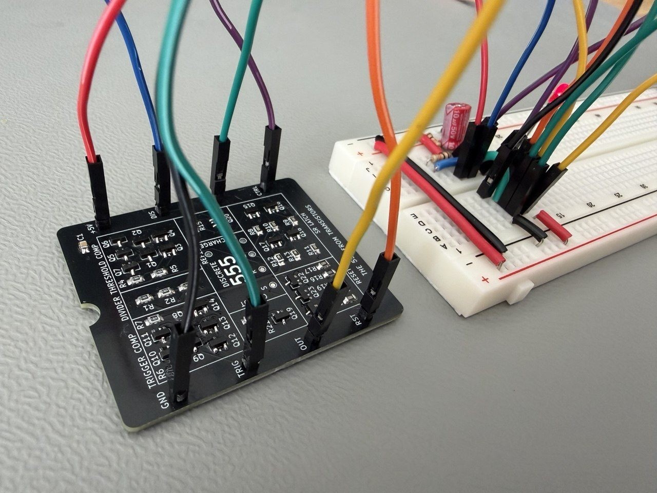
The table gives the eight steps from Figure 14-1 to Figure 14-2.
| Experiment | Step | Result |
|---|---|---|
| 14 · The Master Schematic (this experiment) | Draw the whole circuit on paper, with names and a parts list | The master schematic |
| 15 · Schematic Capture | Enter the master schematic in KiCad | A KiCad schematic with zero errors from the electrical rules check |
| 16 · The Smoke Test | Simulate the KiCad schematic in SPICE | The timing of the design, before a board exists |
| 17 · Going Surface-Mount | Give each part a package | A footprint for each designator |
| 18 · The Board | Place the parts and route the copper | The board layout |
| 19 · Before You Order | Check the design, then order the board | Milestone: the board design is complete |
| The factory makes the board and sends it | Some weeks of waiting | |
| 20 · Assembly Day | Solder the parts on the board | An assembled board |
| 21 · First Power-Up | Apply power with a current limit, then measure | Milestone: the board blinks the LED |
Each step after this one starts from the master schematic. KiCad copies it, SPICE simulates the copy, and the layout draws copper for its nets. The parts list becomes the order. So an error here goes through each step into the copper. On the breadboard, a wrong wire takes a minute to move. On a board, it takes a cut track and an added wire, or a new order.
The board is not an exact copy of the breadboard. This experiment reads the master schematic sheet by sheet, then gives the five places where the board differs, with the reason for each. It needs no power and no instruments.
A breadboard figure names holes, such as 43d, and the names change when a part moves. A schematic names the parts and the connections, and those names stay the same in KiCad and on the board. Each part gets a reference designator: a letter for the type of part and a number. Q is a transistor, R a resistor, C a capacitor, J a connector and TP a test pad. The board has each designator printed beside its part.
A net is a set of terminals that are connected together, so they are at one voltage. A strip of five holes on a breadboard is one net. On a schematic, a net can have a name. Two wires with the same name are connected, even if no line joins them. So the master schematic draws each block on a sheet of its own and joins the sheets by net names, as KiCad does in Experiment 15.
With names for parts and nets, the whole timer fits on one top sheet. The pale outline in Figure 14-3 is the board. Its eight pins are J1, a header with the pin numbers of the NE555. Follow the figure from left to right.
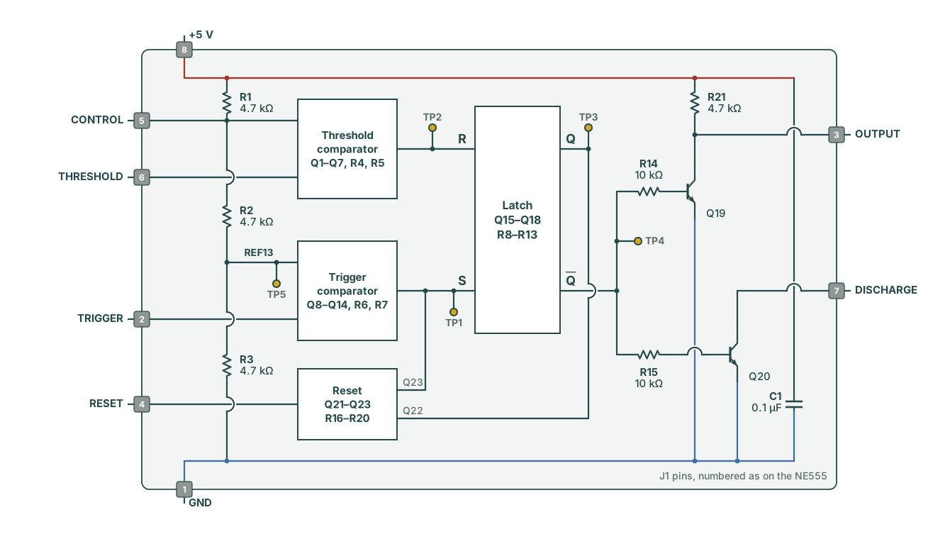
Each box on the top sheet has a sheet of its own, drawn with the layout of the experiment that built the block. The circuits are the same as on the breadboard. In the comparators, four pairs of transistors have each other's names on the board. This page uses the board's names, because they are printed on the board. The table after Figure 14-5 gives both names.
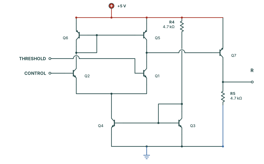
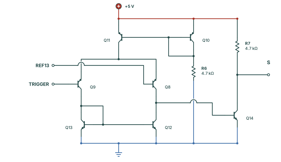
| Transistor | Name on the breadboard | Name on the board |
|---|---|---|
| Threshold pair, base on the 2/3 tap | Q1 | Q2 |
| Threshold pair, base on THRESHOLD | Q2 | Q1 |
| PNP load, diode side | Q5 | Q6 |
| PNP load, side that drives Q7 | Q6 | Q5 |
| Trigger pair, base on TRIGGER | Q8 | Q9 |
| Trigger pair, base on the 1/3 tap | Q9 | Q8 |
| NPN load, diode side | Q12 | Q13 |
| NPN load, side that drives Q14 | Q13 | Q12 |
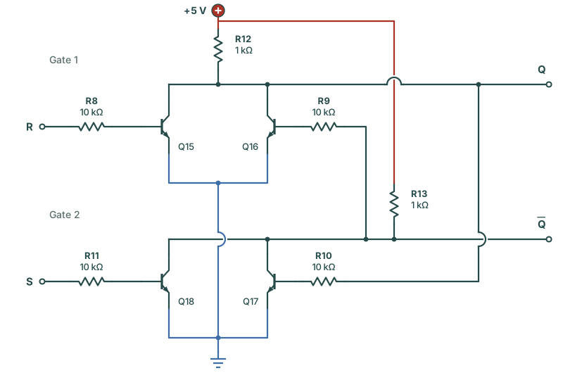
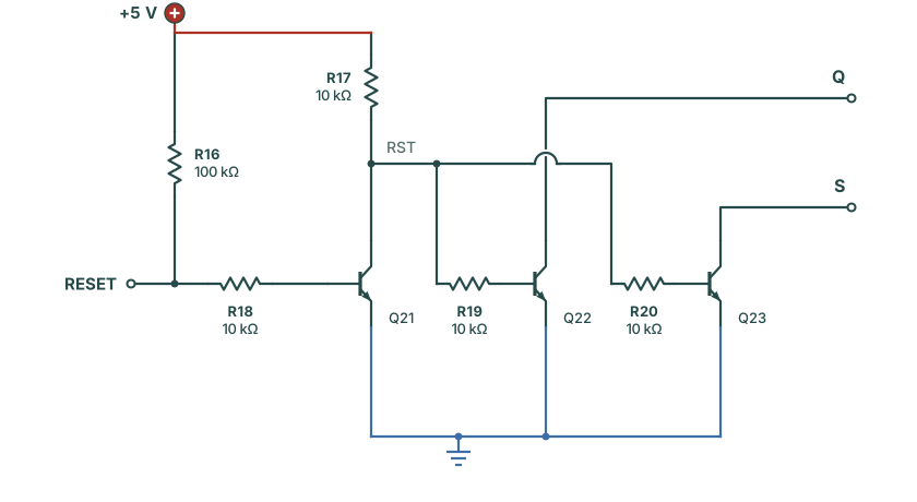
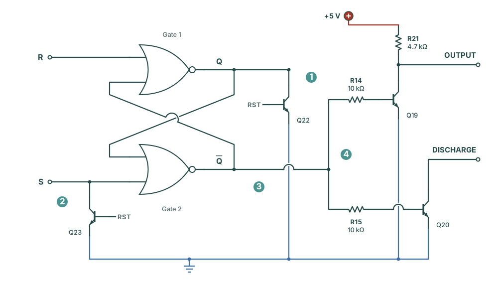
Figure 14-7 has two of the five changes from the breadboard. The top sheet has the other three. The table lists them.
| Change | Breadboard | Board |
|---|---|---|
| Q19's base | Q, through 10 kΩ | Q̄, through R14 |
| Pull-up on OUTPUT | The LED and its 220 Ω | R21, 4.7 kΩ |
| Q23's collector | DIS | S |
| Pull-up on RESET | None: the RESET lead goes in the +5 V rail | R16, 100 kΩ |
| Divider | Three 10 kΩ | Three 4.7 kΩ |
On the breadboard, Q19 takes Q, so its collector is low while C charges, and the LED lights. Pin 3 of the NE555 is high while C charges. On the board, Q19 takes Q̄, so OUTPUT is high while C charges, as on pin 3.
Q19 is an open collector output. It can pull OUTPUT down to 0 V, and it cannot pull it up. On the breadboard, the LED did the pull-up. The board has no LED, so R21 does it. Through R21 the board can supply about 1 mA. The NE555 can supply up to 200 mA from pin 3, as the TI datasheet gives.
With Q19 on Q̄, the reset of Experiment 13 is not sufficient. During a reset, C empties and CAP falls below 1/3, so S rises to 1 and makes Q̄ 0. Q19 turns off, and OUTPUT goes high. The NE555 holds its output low during a reset. So on the board, Q23 holds S at 0. Follow Figure 14-8.
When RESET goes high, Q22 and Q23 turn off, S sets the latch, and C charges from 0 V. That is the long first charge of Experiment 13. Q23 now takes R7's 1 mA, which needs a current gain of about 8. The onsemi datasheet gives at least 100 for the 2N3904.
On the breadboard, the RESET lead goes in the +5 V rail, and a loose lead holds the board in reset. On the board, R16, 100 kΩ, holds pin 4 high. With nothing on pin 4, R16 and R18 give Q21 about 0.04 mA. That turns Q21 on, so the timer runs. A wire from pin 4 to ground resets the timer.
Three equal resistors put the taps at 1/3 and 2/3 for any value, as Experiment 9 showed. The board uses 4.7 kΩ, the value of R4 to R7, so there is one value fewer to buy. The divider current increases from 0.17 mA to 0.35 mA, so the input current of a comparator moves its tap about half as much.
J1 is the only connection to the outside. RA, RB, C and the LED stay on the breadboard, as they stood around the NE555 in Experiment 1. C1 and the five test pads are the other parts that the breadboard did not have.
Each time a block switches, it takes a short pulse of current from +5 V. The supply leads cannot deliver a fast pulse without a short drop on +5 V, and that drop also moves the references of the divider. C1, 0.1 µF, supplies the pulse from beside the circuit. This is called decoupling. Experiment 18 puts C1 beside pin 8.
On the breadboard, each signal between the blocks was on a strip of holes. In Experiments 10 to 13 you put an oscilloscope probe on S, R, Q and Q̄ there. On the board, these nets are copper tracks between SOT-23 legs that are 0.95 mm apart, and J1 has no pin for them. A test pad gives each one a place for the probe tip. The table gives the five pads.
| Pad | Net | What it shows |
|---|---|---|
| TP1 | S | The trigger comparator's output. It is 1 while TRIGGER is below REF13. |
| TP2 | R | The threshold comparator's output. It is 1 while THRESHOLD is above CONTROL. |
| TP3 | Q | The latch output of Gate 1. |
| TP4 | Q̄ | The latch output of Gate 2, which drives Q19 and Q20. |
| TP5 | REF13 | The 1/3 tap of the divider. Pin 5 gives the 2/3 tap, but the 1/3 tap has no pin. |
The pads are on these five nets because the nets are the signals between the blocks. A fault on the assembled board is usually in one block. Compare each block's input with its output, in the order of Figure 14-3, and the first output that is wrong shows the block with the fault.
Each test pad is a round copper pad, 1.0 mm across, on the top of the board. It has no solder mask and no part on it, so it costs nothing and needs no hole. TP1 to TP4 are in one row, so the probe can move from one pad to the next. To use a pad, take the hook off the probe, put the ground clip on pin 1, and hold the probe tip on the pad. A 10× probe puts about 10 MΩ on the net. The resistors that set these nets are 4.7 kΩ or less, so the probe changes the voltage by less than 0.05%.
The test pads are five of the terminals on the named nets. The table lists each named net and all its terminals. A net inside a block has no name on the sheets. KiCad names it from one of its pins, such as Net-(Q1-C).
| Net | Terminals on the net | Pin |
|---|---|---|
| +5V | J1 pin 8, the emitters of the PNP transistors Q5, Q6, Q7, Q10 and Q11, the resistors R1, R4, R7, R12, R13, R16, R17 and R21, C1 | 8 |
| GND | J1 pin 1, R3, R5, R6, the emitters of all sixteen NPN transistors, C1 | 1 |
| THRESHOLD | J1 pin 6, Q1's base | 6 |
| TRIGGER | J1 pin 2, Q9's base | 2 |
| CONTROL | J1 pin 5, the 2/3 tap between R1 and R2, Q2's base | 5 |
| REF13 | The 1/3 tap between R2 and R3, Q8's base, TP5 | – |
| R | Q7's collector, R5, R8, TP2 | – |
| S | Q14's collector, R7, R11, Q23's collector, TP1 | – |
| Q | The collectors of Q15, Q16 and Q22, R12, R10, TP3 | – |
| Q̄ (QB in KiCad) | The collectors of Q17 and Q18, R13, R9, R14, R15, TP4 | – |
| OUTPUT | J1 pin 3, Q19's collector, R21 | 3 |
| DISCHARGE | J1 pin 7, Q20's collector | 7 |
| RESET | J1 pin 4, R16, R18 | 4 |
| RST | Q21's collector, R17, R19, R20. KiCad does not name it. | – |
THRESHOLD and TRIGGER are separate pins. In an astable, they meet outside the board at C, as on the NE555 in Experiment 1.
The nets give the connections, and the parts list gives what to buy. The MMBT3904 and MMBT3906 are the 2N3904 and 2N3906 in the surface-mount SOT-23 package. 0805 is a resistor or capacitor of 2.0 mm by 1.25 mm. Experiment 17 gives each part its footprint.
| Part | Qty | Designators | Package |
|---|---|---|---|
| MMBT3904, NPN | 16 | Q1–Q4, Q12–Q23 | SOT-23 |
| MMBT3906, PNP | 7 | Q5–Q11 | SOT-23 |
| 4.7 kΩ resistor | 8 | R1–R7, R21 | 0805 |
| 10 kΩ resistor | 10 | R8–R11, R14, R15, R17–R20 | 0805 |
| 1 kΩ resistor | 2 | R12, R13 | 0805 |
| 100 kΩ resistor | 1 | R16 | 0805 |
| 0.1 µF ceramic capacitor | 1 | C1 | 0805 |
| Pin header, 1×8, 2.54 mm pitch | 1 | J1 | Through-hole |
| Test pad, 1.0 mm | 5 | TP1–TP5 | Copper on the board |
Before Experiment 15 enters the schematic in KiCad, follow it on paper with a pencil. Print the PDF in the box “Resources” at the top of this page. Each sheet has its figure number in the title block.
Three questions on this experiment. They ask how a net name connects, why Q23 moved to S, and what R16 does.
1. Two wires on two different sheets end in the name S, and no line joins them. They are…
A net is the set of terminals with one name. Every terminal with the name S is on the same net, on each sheet. The board layout then makes the copper for that net.
2. On the board, Q19's base takes Q̄. If Q23 held DIS, as on the breadboard, OUTPUT during a reset would…
C empties during a reset, so CAP falls below 1/3 and the trigger comparator sets S. S makes Q̄ 0, which turns Q19 off. With Q23 on S, S stays 0, Q̄ stays 1 and OUTPUT stays low.
3. Nothing is connected to pin 4 of the board. The timer…
R16 connects pin 4 to +5 V. Current through R16 and R18 turns Q21 on, so RST is near 0 V and Q22 and Q23 are off.
The master schematic gives each part a designator and each connection between the blocks a net name. It lists the parts and records the five changes from the breadboard. That is the first step from the breadboard to the board. The second step is Experiment 15: Schematic Capture, which enters the same sheets in KiCad and checks each connection.