Full Stack Electronics · Stage Three · Experiment 7
Add one PNP transistor and one resistor after the comparator. Its low level then reaches ground at either of the 555's thresholds.
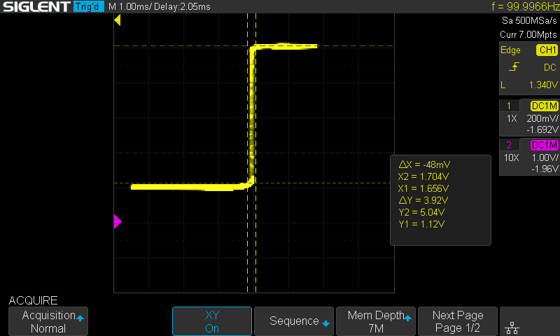
The comparator from Experiment 6 switches within a few millivolts, but its output never gets near ground. Figure 7-1 is its transfer curve from the end of Experiment 6, with V− at 1.67 V. The high level is 5.04 V, and the low level is 1.12 V. In the 555 this comparator watches the upper threshold, 3.33 V, and there the low level is higher again. That matters because the comparator's output goes to logic.
The NOR gates of Experiment 10 take each input through a 10 kΩ resistor to the base of an NPN transistor. That transistor switches on when its input rises above about 0.65 V. So a low level of 1.12 V would switch it on, the same as a high level.
The low level sits about a volt above ground because of the pair itself. Q2 cannot pull its collector below its own emitter. Its emitter sits one base-emitter drop, about 0.65 V, below V−. So the low level follows the reference: when V− rises, the low level rises with it.
Because the low level moves with the reference, this experiment first measures it at 3.33 V. Then it adds an output stage: one PNP transistor, Q7, and one 4.7 kΩ resistor. Q7's emitter is on the +5 V rail, and its base reads the comparator's output. The resistor connects Q7's collector to ground. The comparator's output node, Q2's collector, still decides which input is higher. This page calls that node node A, and the new output is Q7's collector.
Figure 7-1 gives the low level with V− at 1.67 V. The 555 uses this comparator at 3.33 V, so first measure the low level there, before you add anything to the board. The board stays as Experiment 6 left it. V+ comes from the generator at 10j, V− comes from power supply output 2 at 13j, and the probe is on node A at 14i. Only the settings change, so that the comparator works at the 555's upper threshold. Figure 7-2 shows the connections.
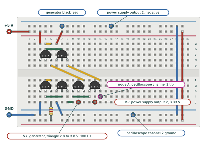
With the leads where Figure 7-2 shows them, change three settings:
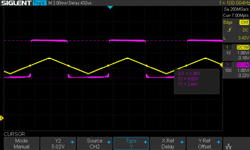
Figure 7-3 is the result. Node A still jumps between its two levels each time V+ crosses 3.33 V. The high level is 5.02 V, close to the 5.04 V at 1.67 V. The low level is now 2.64 V. The reference rose by 1.66 V, and the low level rose by 1.52 V, from 1.12 V in Figure 7-1 to 2.64 V. So the low level follows the reference, and at 3.33 V it is even further from the 0 V that the logic needs.
Figure 7-3 showed that the low level rises with V−. The cause is in the pair, while V+ is below V−. Figure 7-4 shows the comparator with V− at 3.33 V. The tail mirror Q3 and Q4 is drawn as one current-source symbol, labelled tail.
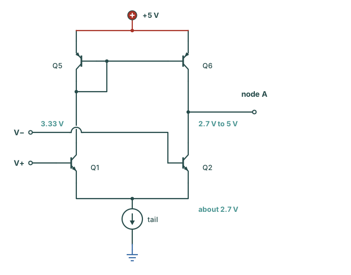
Follow the currents in Figure 7-4 with V+ below V−. Q2 carries the whole tail current and pulls node A down as far as it can. A transistor pulls its collector down only as far as its emitter, within about a tenth of a volt. There it saturates, and the collector stops falling. Q2's emitter is joined to Q1's, and the pair holds that junction one base-emitter drop below the higher input.
With V+ below V−, the higher input is V−. So the emitters sit at 3.33 V minus 0.65 V, about 2.7 V. Node A stops near 2.7 V, and Figure 7-3 reads 2.64 V. At 1.67 V the same sum gives about 1 V, and Figure 7-1 reads 1.12 V.
So Q2's emitter sets the floor, and no change to the load can move it. The output needs a second transistor with its emitter on a fixed rail. That transistor reads node A and drives an output of its own. It can be an NPN or a PNP, and the next section compares the two.
The last section asked for a second transistor. The NPN is the first choice to try, because it is the switch from Experiment 3. Its emitter goes to ground, its base to node A, and a resistor connects its collector to +5 V. Its collector can reach ground. But it switches when its base rises about 0.65 V above its emitter, and node A never falls that far. Figure 7-5 shows the two ranges side by side.
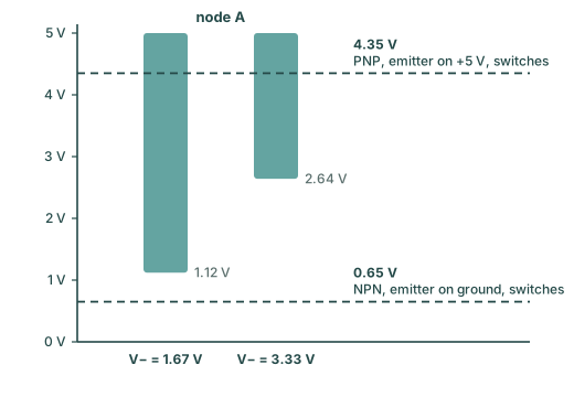
Figure 7-5 shows the problem. The lowest point of node A is 1.12 V or 2.64 V, so the NPN's base would never fall below its switching point. The NPN would be on in both states of the comparator. Its output would stay low whatever the inputs did.
The PNP works the other way round. A PNP with its emitter on +5 V switches when its base falls about 0.65 V below +5 V, near 4.35 V. That point is inside node A's swing at either reference. Experiment 6 already has two PNPs on this rail. A third PNP, Q7, can read node A from the top rail, and its collector can fall to 0 V through a resistor to ground. That PNP and its resistor are the output stage that this experiment builds.
The last section chose the parts. Q7 is a 2N3906 with its emitter on +5 V and its base on node A. A 4.7 kΩ resistor connects its collector to ground. Figure 7-6 shows where they join the comparator, with the parts from Experiment 6 faded. Q7's collector is the new OUT. The 4.7 kΩ resistor is a pull-down: when Q7 is off, it holds OUT at 0 V.
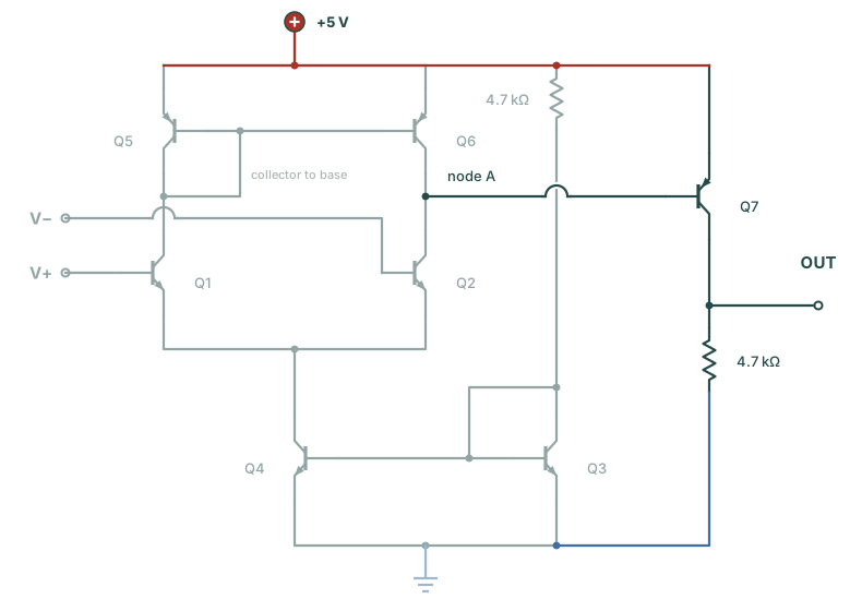
Figure 7-7 puts the same connections on the board. Q7 continues the row of PNPs in the upper block, at 9d to 11d, right after Q6. It stands the same way round as Q5 and Q6, with its emitter on the left. The diagonal jumper from 14f to 8e already brings node A to the upper block, into Q6's collector column, and a short jumper in row b carries it on to Q7's base. The pull-down connects Q7's collector column at 11a to the top ground rail. The probe moves from node A to the same column at 11e.
The whole output stage stays in the upper block. The comparator still spans columns 3 to 14, and both blocks right of column 14 are still free.
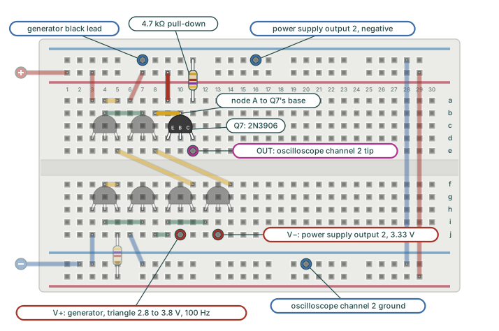
The steps below follow Figure 7-7. Start with the power off.
The next section switches the power on again with the probe at 11e. If OUT then stays at about 5 V whatever the input does, Q7 conducts all the time. Check that Q7 is a 2N3906 and that its flat face points towards the near edge. If OUT stays at 0 V, check the jumper from 9a to the rail and the jumper from 8b to 10b. The pull-down must go to the outer ground rail. On the inner +5 V rail, it would hold OUT high.
Figure 7-3 showed node A stopping at 2.64 V. Now repeat that measurement with the probe on OUT. If the output stage works, OUT falls to 0 V. After that, the same check follows at the lower threshold.
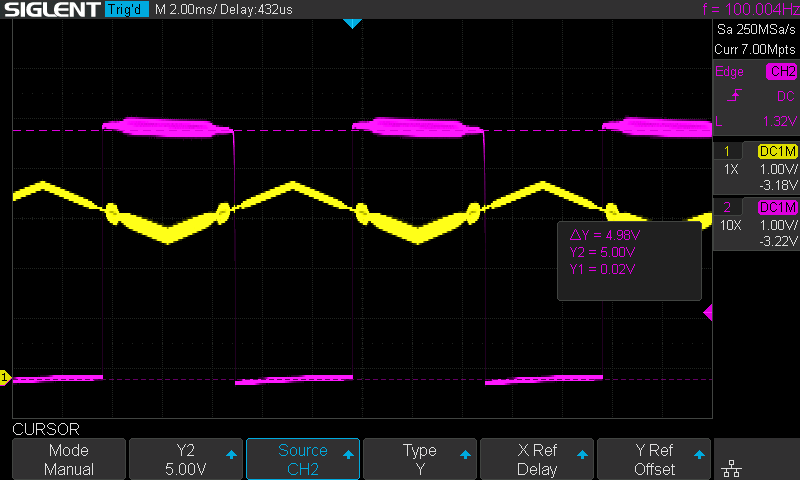
Figure 7-8 is the result. OUT's low level is now 0.02 V, at ground. At the same reference, node A could not fall below 2.64 V in Figure 7-3. OUT is also inverted: it is high while V+ is below V−, and low while V+ is above V−. Experiment 9 uses that when it feeds the signal to V− in place of V+.
Figure 7-8 also shows something that Figure 7-3 did not. While OUT is high, both traces are thick. A fast wobble, much faster than the 100 Hz ramp, appears on OUT's high level and on the ramp. The ramp also has short bursts where OUT switches. In Figure 7-3, before Q7 was fitted, both traces were thin, so the wobble appears while Q7 is on. The cursors still read 0.02 V and 5.00 V through it.
The last section found thick traces while OUT is high. The thick band is an oscillation, far too fast for the 2 ms/div timebase to draw, and the pair makes it itself. While OUT is high, V+ is below V−, so Q2 carries the tail current and its emitters follow its base. Its base connects to power supply output 2 through about a metre of lead.
At tens of megahertz, that lead acts as a small coil. Together with the few picofarads at the emitters, it forms a tuned circuit: a coil and a capacitance that exchange energy at one frequency. A transistor whose emitter follows its base, at the end of such a lead, adds energy to that circuit faster than the wire loses it. So the circuit oscillates. Near the switching points Q1 conducts too, from the generator's lead, and that gives the short bursts on the ramp.
I did not measure the frequency. Figure 7-3 had the same leads and thin traces, so Q7 conducting plays a part too, in a way I did not measure.
A 1 kΩ resistor in series with each base stops it. The oscillating current has to pass through the resistor, which turns more of its energy into heat than the transistor adds, so no oscillation starts. The resistor goes in the base's own column, so that no lead lies between it and the base. Each base draws only a few microamps, so each 1 kΩ moves its input by a few millivolts. From here on, every base that takes a signal from an instrument's lead gets one. Figure 7-9 shows the two on the board.
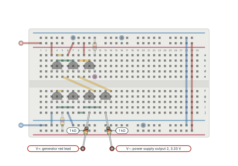
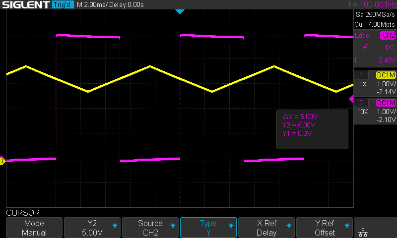
Figure 7-10 is the result. OUT switches at the same place, between the same two levels, and the thick band has gone from both traces.
With the traces clean, the output stage must also work at the 555's lower threshold. There, Figure 7-1 showed a low level of 1.12 V. The reference, the generator and the trigger change.
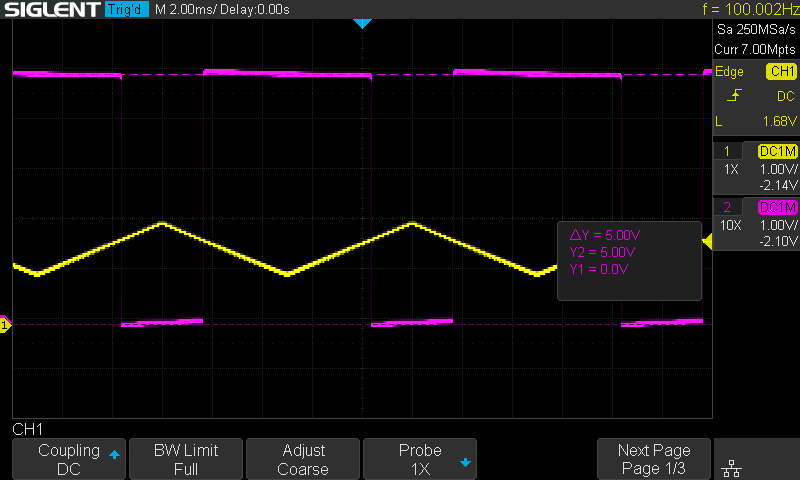
Figure 7-11 shows the same two levels as at 3.33 V. OUT switches where the triangle crosses about 1.7 V, near the new reference. The reference now sets only where OUT switches. The output stage sets how high and how low OUT goes. The table shows the readings before and after Q7 side by side.
| Reference V− | Low level at node A, before Q7 | OUT low | OUT high |
|---|---|---|---|
| 1.67 V | 1.12 V (Figure 7-1) | 0.0 V (Figure 7-11) | 5.00 V (Figure 7-11) |
| 3.33 V | 2.64 V (Figure 7-3) | 0.02 V (Figure 7-8) | 5.00 V (Figure 7-8) |
The table shows what Q7 does to the output. Q2 still cannot pull node A below its floor, yet OUT now reaches 0 V. The reason is that Q7 switches near the top of node A's range, and it stops node A from falling any further. Figure 7-12 marks the steps on the circuit.
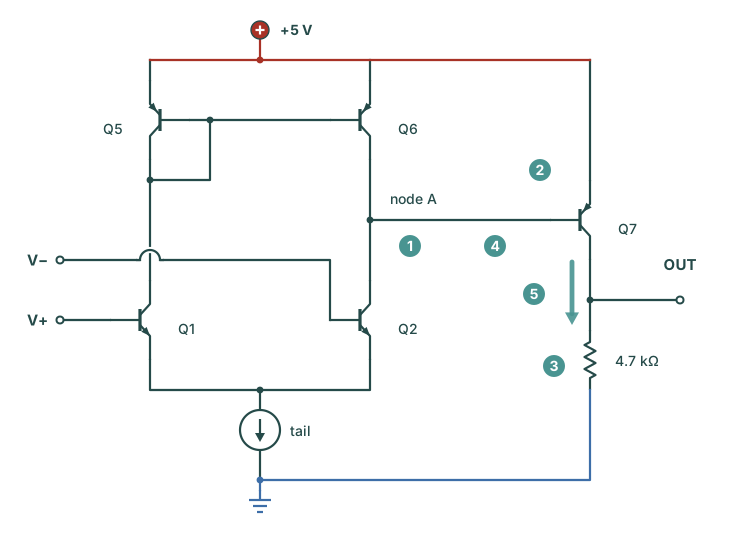
Step 4 says that node A now stops near 4.3 V. You can check that on the board, back at the upper threshold.
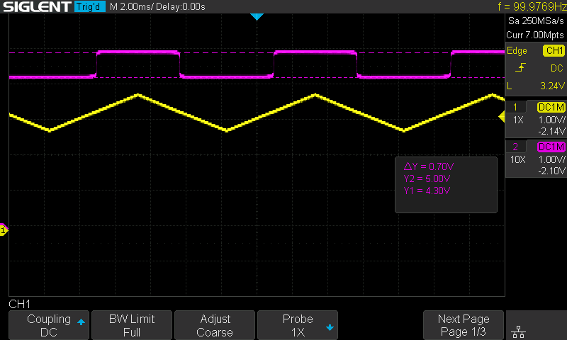
Compare Figure 7-13 with Figure 7-3. Without Q7, node A swung from 2.64 V to 5.02 V. With Q7's base on it, node A swings only between 4.30 V and 5.00 V, a range of 0.70 V. That is Q7's base-emitter drop. Q7 turns that small swing into the full swing of OUT.
This experiment chose a PNP to read a node near the top rail, and the NE555 makes the same kind of choice. In Ken Shirriff's analysis of the chip's die, the threshold comparator works near 2/3 VCC. It has NPN input transistors and a PNP current-mirror load, like the circuit on this board. The trigger comparator works near 1/3 VCC, closer to ground, and it has PNP input transistors. Each stage uses the polarity that suits its voltages. Experiment 8 builds the trigger comparator the other way up.
Flaw 5, the trapped low level, is fixed. Figure 7-3 measured it, and Q7 removed it in Figure 7-8. No flaw joins the list. Power supply output 2 gives V− for now, so that each comparator can be tested on its own. Experiment 9 makes both references on the board, from the 5 V rail.
| # | Flaw | What it means | Found | Status |
|---|---|---|---|---|
| 1 | No reference input | The threshold is the transistor's own 0.6 V. Nothing outside the circuit sets it. | Experiment 3 | Fixed in Experiment 4: the differential pair |
| 2 | Wide transition | The output needs a band of input to travel from high to low: about half a volt with one transistor, about a quarter of a volt with the pair. | Experiment 3 | Fixed in Experiment 6: the active load |
| 3 | Thermal drift | The base-emitter voltage falls about 2 mV per degree, and the threshold falls with it. | Experiment 3 | Reduced in Experiment 4: two matched transistors drifting together |
| 4 | Tail current follows the common-mode level | A resistor tail passes more current as both inputs rise, and the output moves with it. | Experiment 4 | Fixed in Experiment 5: the current mirror tail |
| 5 | Output low trapped a diode drop below the reference | The output's low level sits a diode drop below the reference instead of at ground. | Experiment 6 | Fixed here the PNP output stage |
Three questions on this experiment: why the low level stays above ground, why an NPN output stage would stay on, and how Q7 brings OUT to ground.
1. With V− at 3.33 V and no output stage, node A cannot fall below about 2.7 V because…
Q2 saturates when its collector reaches its emitter. The emitters sit one base-emitter drop below the higher input, so the floor rises with V−.
2. An NPN with its emitter on ground and its base on node A would fail as the output stage because…
The NPN switches when its base rises above about 0.65 V. Node A's lowest point is 1.12 V or 2.64 V, depending on the reference, so the NPN never turns off.
3. With Q7 in place and V+ below V−, node A stops near 4.3 V because…
When node A is about 0.65 V below +5 V, Q7's base supplies Q2's current. Node A stays there, and Q7 switches on hard and lifts OUT.
One transistor and one resistor moved the output's low level from a diode drop below the reference to ground. The comparator is now complete, with seven transistors. The input pair and its tail mirror are NPN, and the active load and the output stage are PNP. It decides within a few millivolts which input is higher. Its output then shows the result at 0 V or 5 V, at either reference. The output is inverted: it is high while V+ is below V−.
This seven-transistor circuit is the 555's threshold comparator, the one that watches 2/3 VCC. The 555 also needs a trigger comparator, which works at 1/3 VCC, nearer ground. Experiment 8: The PNP Twin builds it from the other kind of transistor. It also measures how close to ground this NPN pair keeps working.