Full Stack Electronics · Stage Three · Experiment 6
Replace the pair's collector resistors with a PNP current mirror, and narrow the comparator's switching band from a quarter of a volt to a few millivolts.
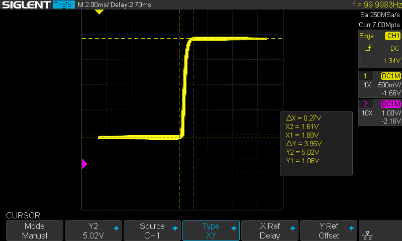
The comparator has one flaw still open from the list in Experiment 3: its output needs too much input to switch. Figure 6-1 is its transfer curve from the end of Experiment 5, the output plotted against V+ with V− at 1.67 V. The output climbed from about 1 V to 5 V while V+ rose from 1.61 V to 1.88 V. A comparator should switch as soon as V+ passes V−, and inside the 555 the timing capacitor charges slowly past each threshold. With a band a quarter of a volt wide, the capacitor voltage spends part of every cycle inside the band. There the output sits between its two levels.
The band is wide because the pair's gain is low. Gain is how far the output moves for each volt of difference between the inputs. Across the step, the rising part of the curve in Figure 6-1, the gain averages about 15: 3.96 V of output for 0.27 V of input. The two 4.7 kΩ collector resistors set that gain, so a narrower band needs a change to them.
A larger resistor is the first idea, and the next section shows what it does to the threshold. The better choice is a second current mirror in place of the two resistors. It uses a new kind of transistor, the PNP. A load made of transistors in this way is called an active load. This experiment introduces the PNP, builds the new mirror onto the board and measures the band again.
On the board, the pair, its mirror tail and the ground and probe leads stay as Experiment 5 left them. You remove two resistors and two jumpers, and you insert two transistors and six short jumpers.
The lead traced the low gain to the two 4.7 kΩ collector resistors. A larger collector resistor would raise the gain, because the same change in Q2's current would make a larger change in the output voltage. On paper, a 100 kΩ in place of the 4.7 kΩ multiplies the gain by twenty. In the circuit, the threshold moves away from V−, and the average gain across the step stays near 40.
Look at the bottom of the step in Figure 6-1. There Q2 carries the whole tail current, about 0.95 mA. Experiment 5's flat output at 2.77 V put 0.47 mA in each side. Through 4.7 kΩ, 0.95 mA would drop 4.5 V and take Q2's collector to 0.5 V, below its emitters at about 1 V. Q2 saturates first, so the low shelf sits at 1.06 V.
A 100 kΩ would need 95 V to pass 0.95 mA. With Q2's emitters near 1 V, the 100 kΩ has about 4 V to drop, so Q2 can pass at most 40 µA before it saturates. With the inputs equal, Q2 takes half the tail, 0.47 mA, so Q2 saturates and the output sits on its low shelf. Q2's current falls to 40 µA only when V+ is about 80 mV above V−. The output leaves the low shelf there and reaches 5 V when V+ is about 180 mV above V−. The theory box below works out these numbers.
So a 100 kΩ still gives a step about 0.1 V wide, but the step sits 80 mV to 180 mV above V−. The resistor and the tail current set that threshold, and V− no longer does. Across the step the gain averages about 4 V ÷ 0.1 V, near 40, the same as before.
A resistor has one number, and it sets two things at once. It sets how far the output moves for a change in current, and how much voltage the steady current drops. The first needs to be large and the second small. No resistor does both. The theory box puts a number on that limit, and the next section describes a load that does both.
The gain of the pair with resistor loads depends on the tail current and the collector resistance only through their product. That product is the voltage the resistor drops when one transistor carries the whole tail current. Double the resistance and halve the current, and the gain stays the same. For the step to stay on V−, that product has to fit between the 5 V supply and the emitters, about 4 V on this board. So the gain at the centre of the step has a cap of about 40, whatever resistor you choose. Experiment 5 worked out a gain near 42 at the centre, so with 4.7 kΩ and 0.95 mA the board is already at the cap.
How steeply one transistor responds. Experiment 5's theory box used the Ebers–Moll model, . The change in collector current per volt of change in base-emitter voltage is the slope of that curve, the transconductance . Differentiate with respect to . The derivative of an exponential is the same exponential, multiplied by the derivative of what is in the exponent, here :
The numerator is itself, so
With 0.47 mA in each transistor and mV, that is about 18 mA/V.
The pair with resistor loads. Let the inputs differ by a small voltage . The current Q1 gains is the current Q2 loses, so the tail node holds still for a difference signal. Q1's base-emitter voltage rises by half of , and Q2's falls by half. Q2's current falls by
The output is 5 V minus the drop across Q2's collector resistor . So less current gives a higher output:
The gain is the change in output divided by the change in input that caused it:
With 18 mA/V and 4.7 kΩ this is about 42.
The cap. Each transistor carries half the tail current at the centre of the step, so put into the gain:
The product is the drop across Q2's resistor when Q2 carries the whole tail, at the bottom of the step. It has to fit between 5 V and the emitters at about 1 V, so it can be at most about 4 V:
With 4.7 kΩ and 0.95 mA the product is 4.5 V, slightly more than fits, which is why Q2 saturates on the low shelf. The current and the resistance appear only as their product, so no choice of resistor raises the cap. A larger gain needs a load that drops little voltage for its steady current and still resists any change in that current.
A larger resistor. The tail current divides between Q1 and Q2 by the 60 mV rule. Q1's base-emitter voltage is higher than Q2's by , so Q1 carries times Q2's current. The two currents add up to the tail current. Solve for :
A 100 kΩ with about 4 V to drop lets Q2 leave saturation at :
The output comes within 0.1 V of 5 V when the 100 kΩ drops only 0.1 V, at :
The step runs from about 80 mV to about 180 mV above V−. The output moves about 3.9 V across those 0.1 V of input, an average gain near 40.
The last section showed that one resistor cannot both drop little steady voltage and resist a change in current. Experiment 5 built a circuit that does both: a current source. A current source passes a set current and lets the voltage across itself settle where the circuit needs it. It needs only a few tenths of a volt to work, and a change in its voltage hardly changes its current. So the plan is to feed each of the pair's collectors from a current source connected to +5 V, in place of the resistor.
Two separate current sources would fail. Their currents would never quite match the pair's, and the mismatch would push the output against a rail. The load current has to follow the pair's current, and a current mirror does that. Its diode-connected side connects to Q1's collector and carries the current Q1 draws. Its other side copies that current into Q2's collector, which remains the output.
Experiment 5's mirror sat on the ground rail and pulled current down. This one sits on the +5 V rail and has to push current down into the pair. That needs transistors of the opposite type, the PNP.
The 2N3906 is the PNP partner of the 2N3904. It comes in the same TO-92 package. With the flat face towards you, its legs read emitter, base, collector from left to right, the same as the 2N3904. Side by side, only the printing tells them apart. Inside, its three layers are stacked in the opposite order, so its voltages and currents run the opposite way.
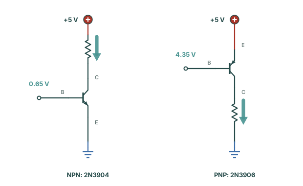
An NPN switches on when its base is about 0.65 V above its emitter, and current flows into its collector and out of its emitter. A PNP switches on when its base is about 0.65 V below its emitter, and current flows into its emitter and out of its collector. So a PNP usually has its emitter on the positive supply and its load below it, towards ground.
Figure 6-2 draws one of each, switched on. The arrow on the emitter shows the direction of the current: out of an NPN, into a PNP. What you learned about the NPN in Experiments 3 to 5 applies to the PNP with the signs reversed. That includes the rule of ten times the current for every 60 mV and the way two of them make a mirror.
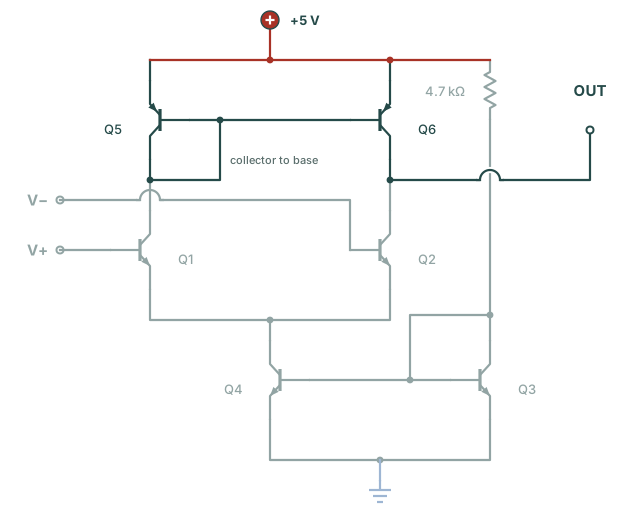
With the PNP introduced, Figure 6-3 shows the whole comparator with the new load. The pair and its mirror tail are drawn faded, as Experiment 5 left them. Q5 and Q6 are the two 2N3906s, with their emitters on +5 V and their bases joined. Q5 is drawn above Q1, with its collector wired to its base. It carries Q1's current, as Q3 carried the reference current in Experiment 5. Q6 is drawn above Q2 and copies that current into Q2's collector, which is still the output.
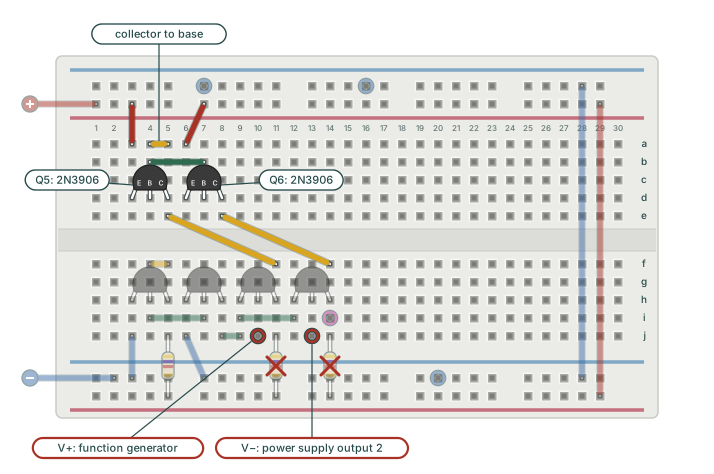
To get from the Experiment 5 board to the circuit of Figure 6-3, first remove the two 4.7 kΩ collector resistors. Figure 6-4 shows them crossed out in red, and the PNP mirror replaces them. I forgot them on my first try, and the circuit still switched, but badly. The caution box below gives the numbers.
Then the two inputs move. The generator's red lead and the positive lead of power supply output 2 go directly onto the base columns, at 10j and 13j. The two jumpers that carried the bases into the upper block are then removed, which clears the centre channel. The PNPs stand in the upper block from column 3, above the tail mirror, both the same way round, with the emitter on the left. Two jumpers run diagonally across the centre channel from the pair's collectors to the PNP collectors.
The whole comparator stays within columns 3 to 14, and the upper block above the pair stays empty. The finished 555 has to fit on this one board, and the space to the right is for the parts still to come. Figure 6-4 shows the board, with everything already built drawn faded.
A 2N3906 looks the same as a 2N3904 and fits the same holes. Read the marking before you insert it. An NPN in Q5's or Q6's place, or a PNP inserted the wrong way round, gives no heat and no smell. The output then stays at one level whatever the input does. If that happens, switch off and check three things: the part number on Q5 and Q6, that both flat faces point towards the near edge, and that both red jumpers reach the +5 V rail.
If the output switches but the step measures tens of millivolts wide, check 11j and 14j first. I left the collector resistors in on my first try. The comparator still worked, which makes the mistake easy to miss, but the step came out about 60 mV wide, a gain of about 65. A 4.7 kΩ left on Q2's collector sits in parallel with Q2 and Q6. Q2 and Q6 together act as about 36 kΩ at the output, so the 4.7 kΩ sets most of the resistance there.
With the mirror built, measure the step again to see how much narrower it is. The measurement is the one from Experiments 4 and 5, with a narrower sweep, so that the ramp passes slowly through the threshold. The generator's red lead is now in 10j. Power supply output 2 holds V− at 1.67 V in 13j. The oscilloscope channel 2 probe is still on the output at 14i.
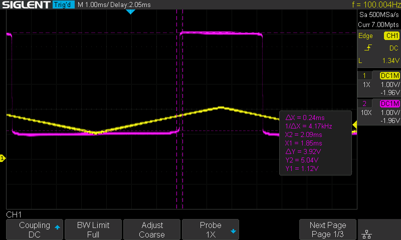
Figure 6-5 is the capture. In Experiment 5 the output ramped between its levels while the input climbed about a quarter of a volt. That ramp has gone. Each edge is now a vertical line at this timebase. The output leaves 1 V and arrives at 5 V while the input barely moves.
The time view shows that the edges are steep, but it does not give their width in input volts. Switch to X-Y mode to see the transfer curve, with input across and output up. Set oscilloscope channel 1 to 200 mV/div with its offset near −1.7 V, so the step sits in the middle of the screen. Place the X cursors on each side of the step and the Y cursors on the two shelves, as in Figure 6-1.
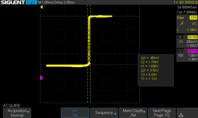
On my board the cursors in Figure 6-6 read 3.92 V of output, from 1.12 V to 5.04 V. On the input axis they sit 48 mV apart, one on each side of the line. So this capture shows only that the step is narrower than 48 mV. Even that means a gain of at least 80, twice the cap of about 40 for any resistor load. To measure the step, return to time across the screen and spread the edge over the whole screen.
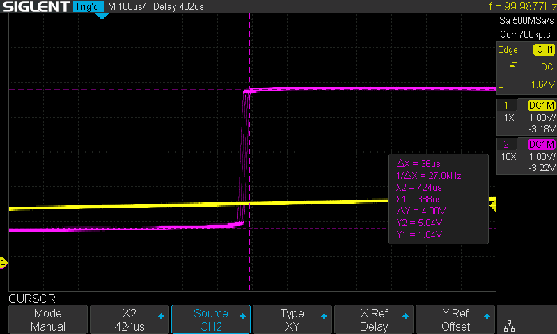
The output takes 36 µs to cross from one level to the other. The input triangle climbs 1 V in 5 ms, which is 0.2 mV every microsecond. So in those 36 µs the input moved about 7.2 mV, and the step is about 7 mV wide. 4.00 V of output for 7.2 mV of input is a gain of about 550. That is nearly forty times the 15 of Experiment 5.
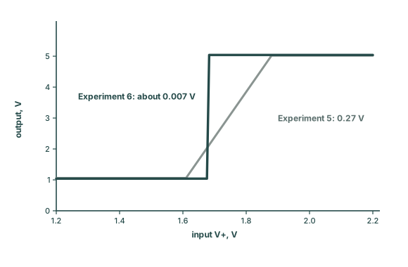
Between them, Experiments 4 and 5 took the step from 0.45 V to about a quarter of a volt. The two PNPs make it about forty times narrower again. The table lists the step at each stage so far.
| Stage | Input step | Output swing | Gain |
|---|---|---|---|
| Experiment 3 · one transistor (Figure 3-6) | 0.45 V | 4.82 V | about 11 |
| Experiment 4 · differential pair (Figure 4-5) | 0.25 V | 3.98 V | about 16 |
| Experiment 5 · mirror tail (Figure 6-1) | 0.27 V | 3.96 V | about 15 |
| Experiment 6 · active load (Figure 6-7) | about 0.007 V | 4.00 V | about 550 |
Figure 6-8 draws the last two rows of the table on one set of axes, from the cursor readings.
The measurements show the step about forty times narrower, and the cause is in how the new load handles current. The active load does two things the resistors could not do. It brings Q1's half of the signal to the output. It also makes the output voltage the only thing that can change to balance any difference in current. Figure 6-9 marks the steps on the circuit. It draws the tail mirror as a single current-source symbol, a circle with an arrow.
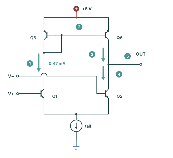
With the resistors, step 5 differed in two ways. First, only Q2's change in current reached the output. Q1's change went into its own 4.7 kΩ and stopped there. Now it comes across through Q5 and Q6, so the output gets twice the change in current. Second, the extra current at the output went into a 4.7 kΩ, which turned each microamp into 4.7 mV.
Now only Q2 and Q6 themselves can absorb extra current at the output. Each of them passes slightly more current as the voltage between its collector and emitter grows. Experiment 5 called this the Early effect. The output voltage has to move tens of millivolts before that tilt absorbs one extra microamp. In Experiment 5 the same tilt made the mirror's copy a few per cent high, a small error in a current. Here it sets the gain of the whole comparator.
The two effects multiply. Bringing Q1's half across doubles the change in current at the output. The resistance that current meets at the output depends on how much Q2's and Q6's currents tilt with their collector voltages. On this board it works out at about 36 kΩ, in place of 4.7 kΩ. Together the two effects raise the gain at the centre of the step from about 42 to about 640, a factor of fifteen.
The board gives about 550 in Figure 6-7, close to that estimate and about 14 % below it. At that gain the full 4 V of output needs only about 7 mV of input. The derivation below works through the numbers.
The current arriving at the output. Let the inputs differ by a small voltage . As in the theory box on resistor loads, the tail node holds still. Q1's current rises by , and Q2's falls by the same amount. Q5 carries Q1's current and Q6 copies it, so Q6 pushes more into the output wire. Q2 takes less out of it. The extra current arriving at the output is the sum:
The tilt of a transistor's current. Experiment 5's derivation added the Early effect to the model, . Hold the base-emitter voltage steady and change only the collector-emitter voltage. The current changes by
The approximation drops the small factor . The inverse of this slope is a resistance, the transistor's output resistance:
Where the output settles. Let the output rise by . Q2's collector-emitter voltage rises by , so Q2 takes more current out of the output wire. Q6's emitter is on +5 V and its collector on the output, so its collector-emitter voltage shrinks by . Q6 then pushes less in. The output stops moving when these two changes together cancel the extra current:
The bracket is the conductance of the two output resistances in parallel, . Solve for :
The gain is divided by :
The numbers. Experiment 5 took the Early voltage of a 2N3904 to be of the order of 100 V. The 2N3906's is lower. Widely used simulation models put it near 20 V. With 0.47 mA in each transistor:
Two resistances in parallel combine as their product over their sum:
With resistor loads the gain was . The ratio of the two is . The 2 comes from bringing Q1's half across, and the rest from the higher resistance at the output.
The Early voltages vary from one transistor to the next. The 100 V for the 2N3904 is an order of magnitude. The 20 V for the 2N3906 comes from simulation models, so 640 is only an estimate. The board's 550 is about 14 % below it.
The circuit now on the board is a differential pair with a mirror as its tail and a second mirror as its load. It is the input stage of many op-amps and comparators. The µA741, the op-amp Dave Fullagar designed at Fairchild in 1968, is still one of the best known. Its input stage has a current-mirror load, which does the same two jobs there. It carries both halves of the pair's signal onto one wire, and it gives far more gain than a resistor that fits on the supply. On a chip, matched transistors take little area, and a large resistor takes a lot.
At this gain the output sits between its two levels only while V+ and V− are within a few millivolts of each other. Everywhere else it rests at about 1 V or about 5 V, which is the comparator working. A difference between Q5 and Q6, or between Q1 and Q2, moves the threshold a few millivolts away from V−. Keep each matched pair touching, so the two transistors share a temperature. That keeps the shift small.
The flaw list opened in Experiment 3 with three flaws. Experiment 4 added a fourth, and Experiment 5 fixed it. The active load fixes the wide transition, the last flaw from Experiment 3 still open. One flaw joins the list here: the output's low level sits about a diode drop below V−. It stays open until Experiment 7.
| # | Flaw | What it means | Found | Status |
|---|---|---|---|---|
| 1 | No reference input | The threshold is the transistor's own 0.6 V. Nothing outside the circuit sets it. | Experiment 3 | Fixed in Experiment 4: the differential pair |
| 2 | Wide transition | The output needs a band of input to travel from high to low: about half a volt with one transistor, about a quarter of a volt with the pair. | Experiment 3 | Fixed here the active load |
| 3 | Thermal drift | The base-emitter voltage falls about 2 mV per degree, and the threshold falls with it. | Experiment 3 | Reduced in Experiment 4: two matched transistors drifting together |
| 4 | Tail current follows the common-mode level | A resistor tail passes more current as both inputs rise, and the output moves with it. | Experiment 4 | Fixed in Experiment 5: the current mirror tail |
| 5 | Output low trapped a diode drop below the reference | The output's low level sits a diode drop below the reference instead of at ground. | Found here | Open until Experiment 7 |
The low level in Figure 6-6 is still about 1.1 V, a volt above ground, the same as with the resistors in Figure 6-1. Q2 cannot pull its collector below its emitters, and the emitters sit about 0.65 V below V−. The logic this comparator drives in the 555 needs a low level near 0 V. Experiment 7 adds an output stage for that.
Set V− to 3.33 V, the 555's upper threshold. Move the generator's triangle up so that it crosses 3.33 V, from 2.8 V to 3.8 V for example. In X-Y mode, set oscilloscope channel 1's offset near −3.3 V. The low level should sit about 0.65 V below V−, near 2.7 V, because Q2 cannot pull its collector below its emitters. Note the reading, because Experiment 7 starts from it.
1. A 100 kΩ collector resistor in place of the 4.7 kΩ would not make a better comparator because…
A resistor's value sets both its gain and its steady voltage drop. With about 4 V to drop, a 100 kΩ passes at most 40 µA. Q2 stays saturated until V+ is about 80 mV above V−, so the threshold moves away from V−. The average gain across the step stays near 40.
2. With the active load, a millivolt of extra input moves the output much further because…
The mirror holds its current, and so does Q2. Neither absorbs extra current at the output except through the small change of current with collector voltage. That acts as tens of kilohms in place of 4.7 kΩ.
3. With resistor loads, Q1's change in current was lost. With the active load it…
Q5 carries Q1's current, and Q6 copies it onto Q2's collector. When Q1 takes more and Q2 less, both changes push the output the same way.
You removed two resistors and inserted two PNP transistors and six jumpers, and the step went from 0.27 V wide to about 7 mV. The comparing part of the comparator is now done. Six loose transistors tell which of two voltages is higher to within a few millivolts. They form a differential pair with a mirror for its tail and a mirror for its load. For the 555 that is enough. The timing capacitor travels 1.67 V between the two thresholds, and 7 mV is under half a per cent of that.
The resistors could not reach this because their value set both the gain and the voltage they dropped. The PNP mirror drops only the voltage it needs and holds its current. So any imbalance between the pair's two halves can only change the output voltage. The mirror also brings Q1's half of the signal across to the output, which the resistors wasted.
The output stage is still missing. The output's low level sits a volt above ground and follows V−, and the logic it drives needs a low level near 0 V. Experiment 7: The Output Stage adds one transistor that takes the output down to ground, and with it the comparator is complete. The 555 also needs a second comparator, the trigger comparator. Experiment 8: The PNP Twin builds it and measures where the NPN pair stops working.