Full Stack Electronics · Stage Two · Experiment 2
Build the timer from separate blocks, then see why its output needs a driver.
In Experiment 1, you built a blinker and measured its output and capacitor voltage. Now you build a similar timer from two chips, resistors and transistors. You can probe the connections between its blocks and see how they work together.
We connect and check the blocks one at a time. Experiments 3 to 11 then rebuild the comparators, the divider and the latch from transistors and measure each one.
Use a second breadboard and a second set of timing parts, so the reference 555 stays assembled. The timing resistor and capacitor values match Experiment 1. Individual components can still differ within their tolerances.
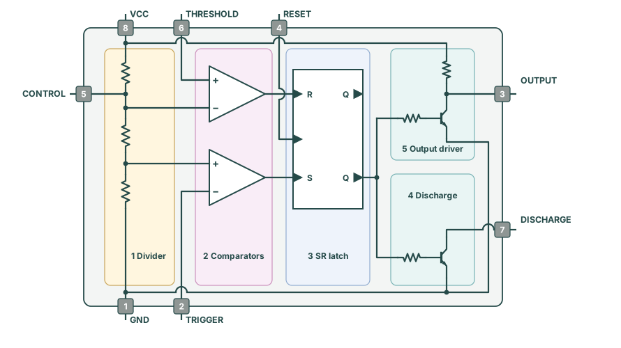
Inside the 555 timer, five functional blocks charge and discharge an external timing capacitor and switch the output. In this experiment, you rebuild those blocks on a breadboard and measure what each one does.
The schematic grows with the breadboard. Each new stage appears beside the existing parts, which the figures show pale. We build the divider, the comparators and the latch first. Then we add the two branches on the right: the discharge transistor, which completes the timing loop, and the output driver, which lights the LED.
A voltage divider produces two reference voltages. A pair of comparators, grouped as one block, compares the capacitor voltage with those references. A latch stores whether the capacitor should charge or discharge. A discharge transistor switches the capacitor's discharge path, and an output driver supplies current to the LED.
We rebuild the timing loop shown in the NE555 datasheet. The blocks sit spread out on a breadboard, so you can measure what happens between them. This experiment uses comparator and logic chips. Later experiments build those blocks from transistors, and Experiment 13 adds the reset input.
Figure 2-1 starts with the divider at the left. The divider gives the timer two fixed voltages to compare with the capacitor voltage. I want you to measure these first, while the board holds only three resistors and the supply wiring.
A voltage divider is a chain of resistors connected across a supply. When nothing else draws significant current from the junctions, the same current flows through all three resistors. Equal resistances therefore have equal voltage drops: each takes one third of the supply voltage.
Count from ground upwards. The first junction is one resistor above ground, so it sits at ⅓ of the supply. The next junction is two resistors above ground, so it sits at ⅔ of the supply. At 5.00 V, expect about 1.67 V and 3.33 V. The equal resistors set these ratios. We use 4.7 kΩ for each.
Disable the power supply outputs before you add, move or remove a component or test jumper. If a power supply output enters constant-current mode, or a part becomes hot, disable the outputs. Then check the wiring. Connect the electrolytic capacitor's striped negative lead to ground. Connect the oscilloscope ground clips only to ground. A ground clip on a signal or on the positive rail can short that point to ground.
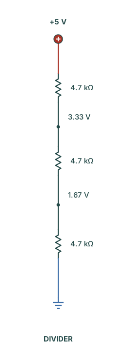
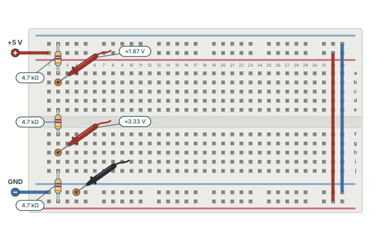
The divider is now assembled. Before you connect anything to its two references, check that it divides the supply as expected. Use the multimeter to measure the supply, then each junction relative to ground. These three readings show whether the next block receives the reference voltages it needs.
Small differences are normal, because the resistors have tolerances. If either reading is near zero or near the full supply, disable power supply output 1 and check the chain and the rail links. Holes a–e in each numbered column connect together. Holes f–j in the same column form a separate group. The two leads of a resistor must reach different groups.
Before you add the next block, you should have two steady reference voltages, about 1.67 V and 3.33 V. Disable power supply output 1 and leave the divider in place.
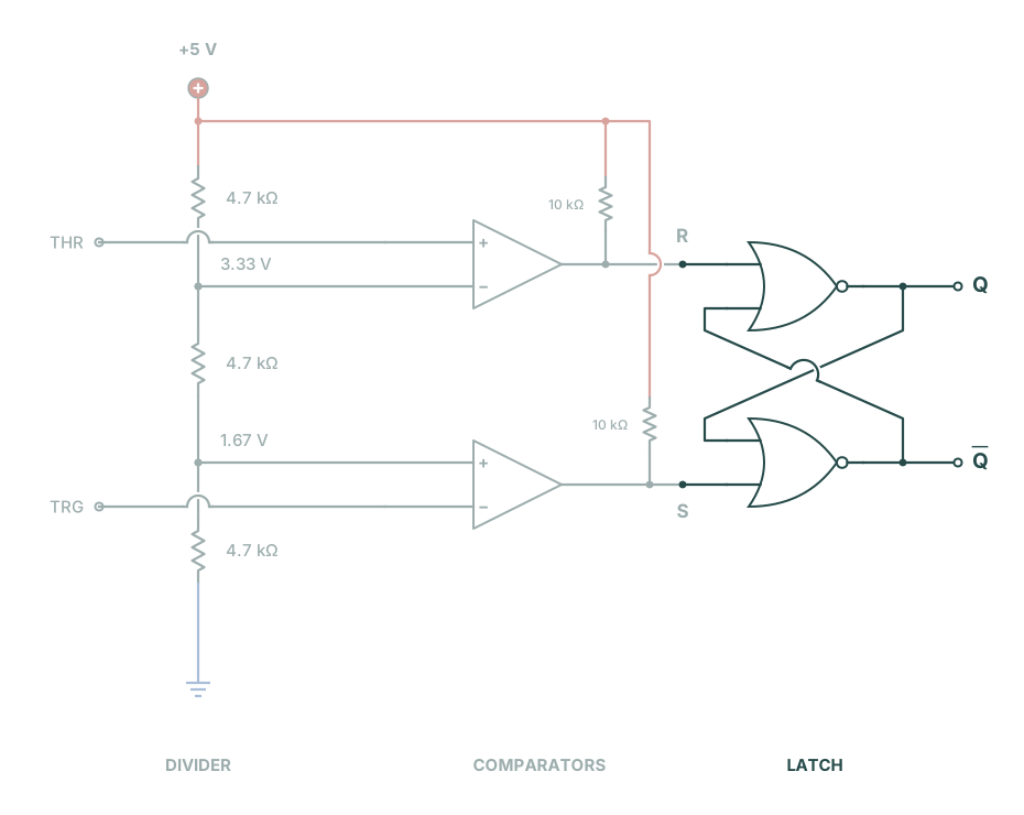
The divider gives two steady references, about 1.67 V and 3.33 V. The comparators use them to detect two conditions. TRG (trigger) below 1.67 V starts charging, and THR (threshold) above 3.33 V starts discharging. The two comparators in the LM393 make these comparisons.
In our timer, TRG and THR both watch the same timing capacitor. Each comparator sends its result to the latch, which we add next.
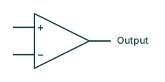
A comparator compares its + and − inputs. With the pull-up resistor described below, its output is high when + is higher than −, and low when + is lower than −. Its output changes whenever the two inputs swap order, and keeps its level while their order stays the same.
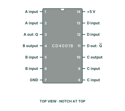
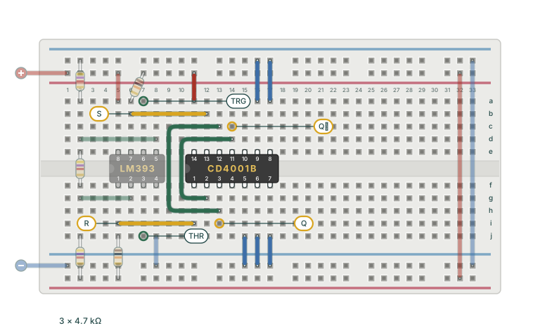
Use the LM393 pinout in Figure 2-4 to identify the supply pins, inputs and outputs. The breadboard drawing turns the chip so its notch faces left.
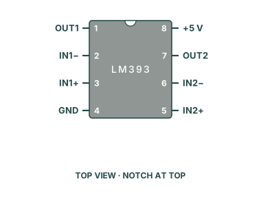
Each LM393 open-collector output contains a transistor that can pull its pin low. When that transistor is off, a pull-up resistor connects the pin to +5 V. We fit one 10 kΩ pull-up to each output, so each output gives a defined high as well as a low.
The references are ready, and the pull-ups give each output a clear high or low. Keep the divider in place, and add the LM393 and its two pull-ups as Figure 2-5 shows. Connect the reference inputs now. Leave TRG and THR free, so you can test each comparator before you fit the timing capacitor.
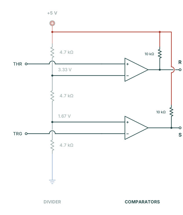
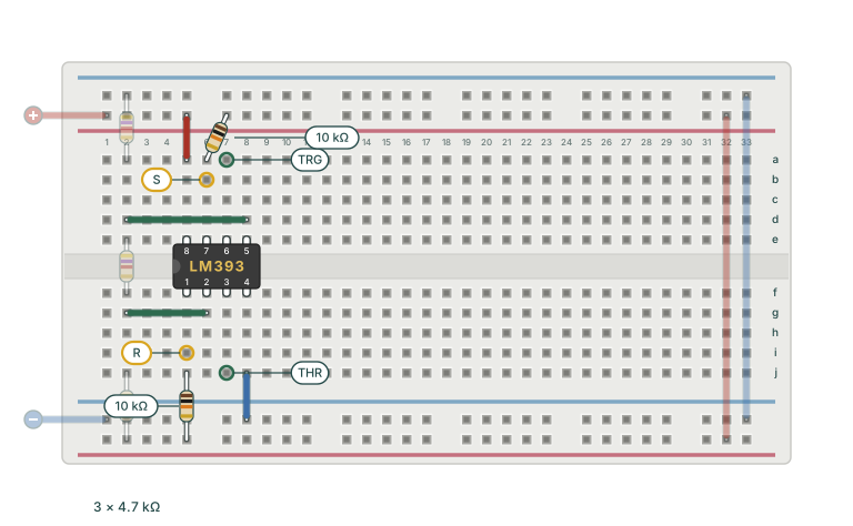
The LM393 now has its references and pull-ups. Keep these tests near room temperature and at or below 3.40 V. The original LM393 does not accept every voltage up to its positive supply as a valid comparison input. At a 5 V supply, TI specifies an input range up to 3.5 V at 25 °C. Across the full rated temperature range, the limit is 3.0 V. Our 3.33 V threshold is therefore a room-temperature bench demonstration. TI does not guarantee this circuit across that full temperature range.
Keep the board on power supply output 1 at 5 V. Use power supply output 2 for the test voltage, in independent mode (each output set on its own, with no series or parallel tracking selected). Connect the negative terminal of power supply output 2 and the multimeter's black probe to the bottom blue rail.
Test the trigger comparator first. Connect the positive terminal of power supply output 2 to TRG at 7a. Enable power supply outputs 1 and 2, and measure S at 6b with the multimeter. At 1.50 V, below the 1.67 V reference, S should read near 5 V. At 1.80 V, above the reference, S should read near 0 V.
Then test the threshold comparator. Disable power supply outputs 1 and 2. Move the output 2 test lead to THR at 7j. Enable both power supply outputs again, and measure R at 5i with the multimeter. At 3.20 V, below the 3.33 V reference, R should read near 0 V. At 3.40 V, above the reference, R should read near 5 V.
After the tests, disable power supply outputs 1 and 2, and disconnect power supply output 2 from the board.
Each comparator output switched at its reference in the tests above. Later, both comparator inputs connect to the timing capacitor. Below 1.67 V, the trigger comparator makes S (set) high to start charging. Above 3.33 V, the threshold comparator makes R (reset) high to start discharging. Between these two limits, S and R are both low (near 0 V), and neither comparator tells the circuit to change state.
That is why the timer needs a latch: a circuit that remembers its last state. While S and R are both low, the latch keeps the capacitor charging if it was charging, or discharging if it was discharging. The next comparator output to go high changes that state.
A NOR gate follows one rule: its output is high only when both inputs are low. Here, low means near 0 V and high means near +5 V. We write these as 0 and 1. The CD4001B contains four NOR gates, and we use gates A and D.
In this latch, each gate's output feeds an input of the other gate. These crossed wires provide feedback: each output helps hold the other gate's state. The four pictures show S going high and then low, followed by R going high and then low. Each picture shows the signals after the gates settle.
1 = high (near +5 V) · 0 = low (near 0 V)
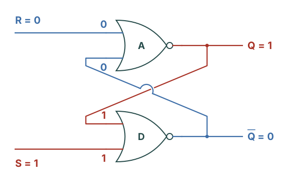
S rises → Q̅ falls → Q rises. D has a high input, so its output is low. A now has two low inputs, so its output is high.
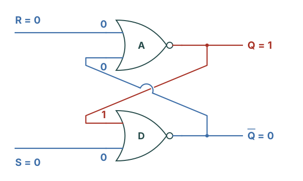
Q stays 1. Follow its high back into D: it keeps Q̅ low. Follow Q̅ back into A: two low inputs keep Q high.
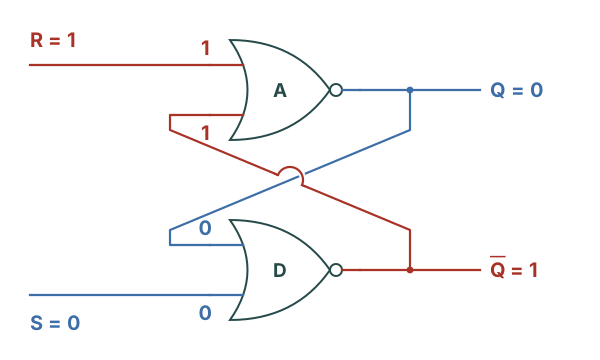
R rises → Q falls → Q̅ rises. A has a high input, so its output is low. D now has two low inputs, so its output is high.
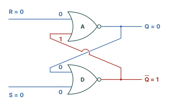
Q stays 0. The high on Q̅ keeps A's output low. That low feeds D, whose two low inputs keep Q̅ high.
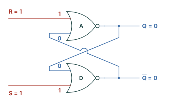
Both gates have a high input, so both outputs become 0. Avoid this combination. If S and R then fall together, the final stored state is unpredictable.
The latch needs power to keep its state. At power-up, apply set or reset to give it a known state.
In our timer, the trigger comparator supplies S and the threshold comparator supplies R. Between the two voltage limits, both are low, so the latch holds its state. Q̅ controls the discharge transistor, which we add next. When Q̅ is high, the transistor is on and the capacitor discharges. When Q̅ is low, the transistor is off and the capacitor charges.
The manual checks show the two states. Once the timing loop runs, the latch holds each state while the capacitor voltage moves between the references. The next section adds the transistor that Q̅ controls.
The latch set and reset as expected in the manual checks. The schematic now extends from Q̅, the latch output at 14c on the breadboard (CD4001B pin 11). A 10 kΩ resistor connects Q̅ to the base of the discharge transistor. The divider, comparators and latch keep their places in Figure 2-9. The new parts appear on the right.
DIS is the junction of the two timing resistors and the transistor's collector. It matches DISCHARGE, pin 7 of a 555. TRG/THR is the capacitor's positive terminal. The return wire from TRG/THR connects to both comparator inputs, so the comparators monitor the capacitor voltage. The bottom blue line joins the capacitor and transistor to the divider’s ground. The pinouts and breadboard layouts show the IC pin numbers and supply wiring.
Short solid-core wire connects everything inside the dashed boundary. Three connections cross the boundary: DIS, TRG and THR. A 555 brings these out as pins, so the breadboard uses tagged jumper leads for them. The tags keep the chip’s inputs and outputs visible in the layout.
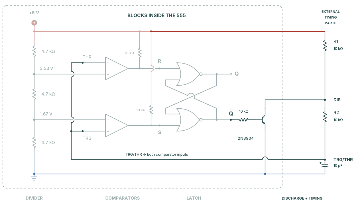
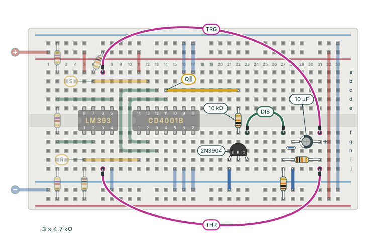
The timing loop is now complete. The capacitor feeds the comparators, the comparators control the latch, and the latch controls the discharge transistor. Until now, you checked individual blocks. This test shows whether they work together and repeat the charge and discharge cycle on their own.
Watch two signals together on the oscilloscope: the capacitor voltage at TRG/THR and the latch output Q. Side by side, they show whether Q changes state at the capacitor's upper and lower limits. Then measure those limits and the time for one cycle, as you did with the reference 555.
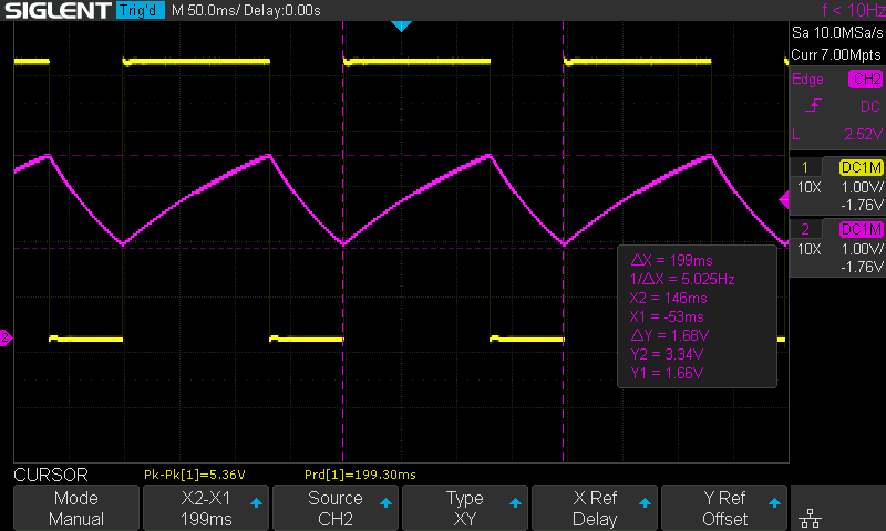
Expect TRG/THR to rise from about 1.67 V to 3.33 V, then fall to 1.67 V again. Q should be high during the rise and low during the fall. The capacitor charges through R1 and R2 and discharges through R2 alone, so the rise should last about twice as long as the fall.
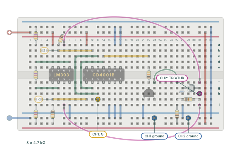
If the capacitor stays low, check that the discharge base resistor goes to pin 11 (Q̅). A base wired to pin 3 (Q) holds the transistor on during the charge, and the capacitor stays at ground. If the capacitor stays high, check the discharge transistor's pinout and the threshold comparator wiring. If neither signal changes, check the chip power, the two pull-ups and the latch feedback. Disable power supply output 1 before each correction. For an unexpected voltage, check the cursor source and probe settings before you change the circuit.
Figure 2-12 shows the loop running. Here is one cycle on your board, step by step.
The loop runs on its own: Figure 2-12 shows one cycle every 199 ms, with Q high through each charge. The other branch after the latch supplies current to a load. Before you add its transistor, measure what happens when the latch drives the LED directly.
Add a load to Q and measure its effect on Q's high level. Leave both probes where they were: oscilloscope channel 1 on Q, oscilloscope channel 2 on TRG/THR. This short test checks how much current the CD4001B can supply. The oscilloscope shows the result.
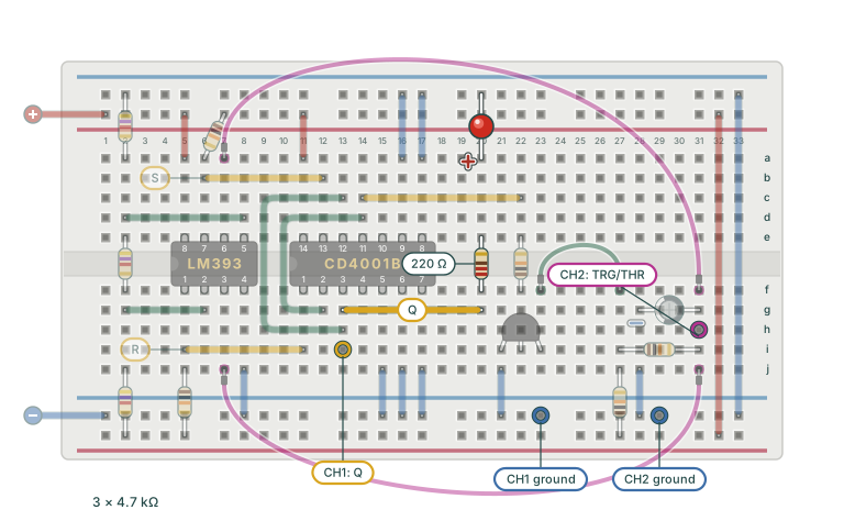
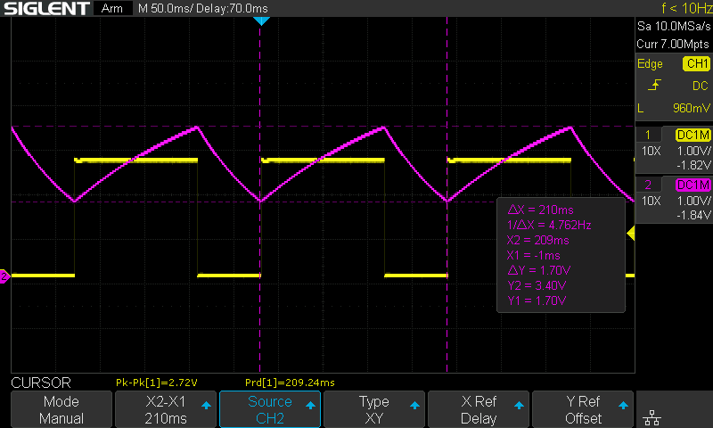
These are my recorded values. Treat them as a guide, because the LED type, component tolerances and measurement setup all shift the readings.
In Figure 2-14, Q's high level fell to about 2.6 V. The CD4001B can supply some output current. This LED and its 220 Ω ask for more current than the gate can supply while its output stays near 5 V. A loaded latch output may also stop being a reliable high for the other NOR gate. Other logic families and lighter LED loads can behave differently.
Q's high level fell with the LED connected, so the LED gets its own transistor. With a second NPN transistor, the supply provides the LED current and Q supplies only a small base current. This transistor is a grounded-emitter switch, like the discharge transistor. Its base connects to Q through 10 kΩ, and its emitter connects to ground. The LED and its 220 Ω connect from +5 V to its collector. When Q is high, the transistor is on, pulls the collector low and lights the LED.
This output stage suits our LED load. It shows why a separate driver between the latch and the load helps. It does not copy the complete output stage of the NE555.
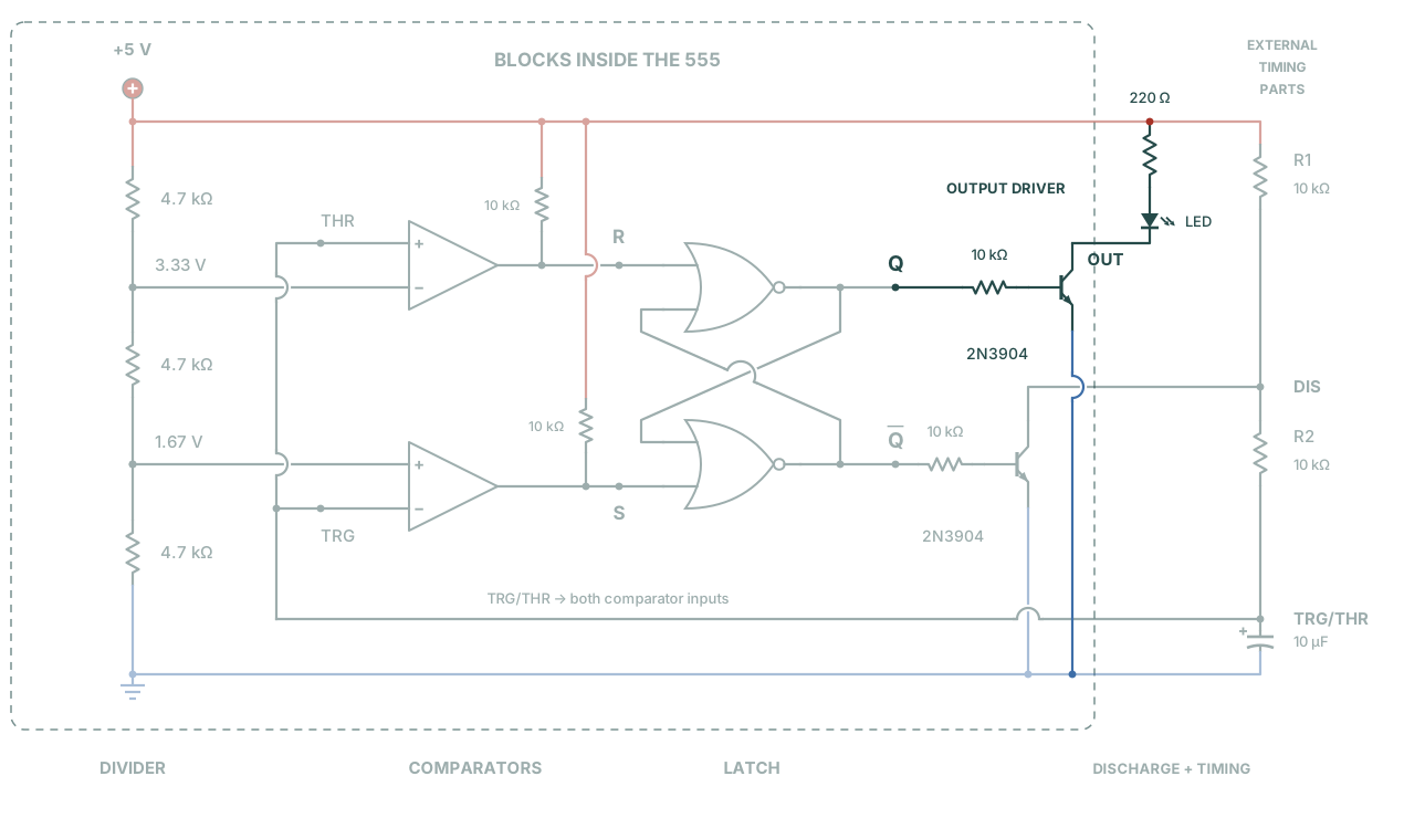
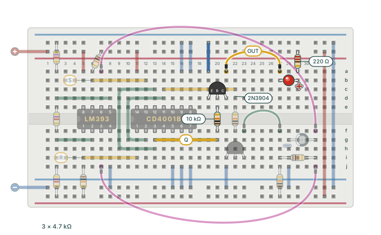
OUT is the opposite of Q because a grounded-emitter stage inverts: a high at the base pulls the collector low. OUT is therefore low while the capacitor charges and high while it discharges. That is upside down relative to pin 3 of an NE555. In Stage Four, the master schematic of Experiment 14 moves this transistor's base to Q̅. The inversion then turns Q̅ back into Q at OUT.
When the transistor is on, it holds OUT near ground. When it is off, the LED and 220 Ω give a weak pull-up path. The measured high level depends on the LED’s current–voltage characteristic and on the load, including the oscilloscope probe. This output drives the LED, and its high level has no specified logic value.
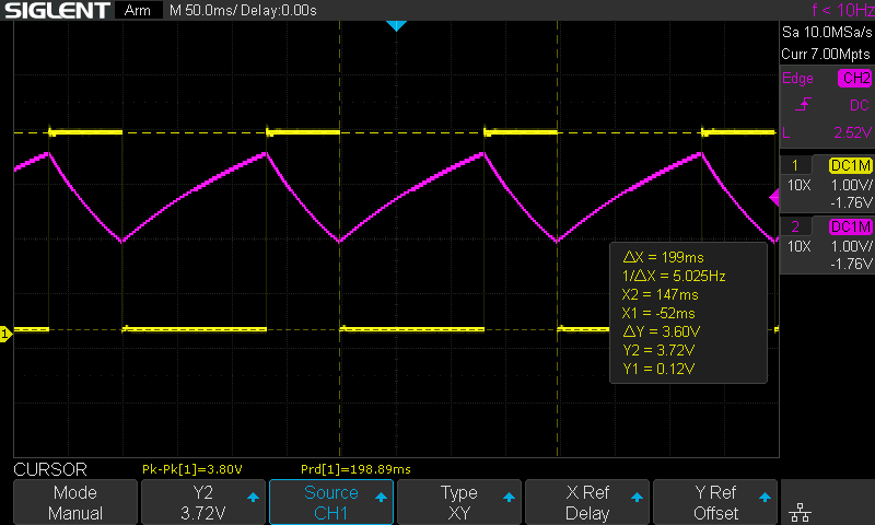
With the driver fitted, Q's high level recovered, and Figure 2-17 shows the same 199 ms cycle as Figure 2-12. The table compares that rate with the formula and the reference chip.
| Formula or build | Frequency |
|---|---|
| Formula, with 10 kΩ, 10 kΩ and 10 µF | 4.81 Hz |
| My NE555 reference (Experiment 1) | About 4.98 Hz |
| My IC timer, with the output driver | About 5.02 Hz |
With the driver fitted, the IC timer runs about 4.5% above the formula and within 1% of the reference chip. The same nominal R and C values and the same one-third and two-thirds thresholds explain the similar timing. The match is close but inexact. Component tolerances, the actual switching levels and the discharge transistor's on-state voltage can all contribute to the difference.
The direct LED test in Figure 2-14 measured 4.78 Hz while Q carried a heavy load. The driver measurement is closer to the reference. These captures alone do not show how much of the frequency difference came from the load and how much came from other changes between measurements.
Compare your two boards with the same oscilloscope settings. Record the IC timer's period, frequency and capacitor limits with the driver fitted. Record Q's low and high levels too. The check is that the loop oscillates near the rate the formula gives. The exact figure depends on your parts and their switching levels.
You built a 555 from off-the-shelf parts. A three-resistor divider sets the two references. The LM393's two comparators watch the capacitor against them. The CD4001B provides the latch's two NOR gates. One transistor discharges the capacitor, and a second drives the LED. Together they charge and discharge the capacitor and blink the LED near 5 Hz, the same loop the reference chip ran in Experiment 1.
The five blocks of Figure 2-1 now run on your bench. Stage Three rebuilds each of them from individual transistors, starting in Experiment 3.
1. Why does this timer need a latch?
Between the references, both comparator outputs are low. Feedback in the latch keeps the last state until set or reset requests a change.
2. Why does each LM393 output need a pull-up resistor?
The pull-up supplies a defined high when the open-collector output transistor is off. When that transistor conducts, it pulls the output low.
3. What changes when you add the output driver?
The two transistors have separate jobs. One switches the LED current. The other controls the capacitor's discharge path. Both still need their base resistors.
Keep this board assembled beside the NE555 reference. Save an oscilloscope capture. Record the probe points, the supply voltage and your measurements. Experiment 12 compares these boards with the transistor timer.
Experiment 3 starts with one transistor and develops it into a comparator, step by step. If you get stuck, you can ask me at @dnixty. A board photo, your probe points and your measurements help me answer.
Component references: LM393 datasheet, CD4001B datasheet, and onsemi 2N3904 datasheet.