Full Stack Electronics · Stage Four · Experiment 19
The sixth step from the breadboard to a printed circuit board. Check the board in the ways that the design rules checker cannot, write the files for the factory, check those files, and order the board.
Experiment 18 ended with the design rules checker at zero. The checker compares the board with rules and with the schematic. It does not see three things. It does not see what is wrong but legal, such as a pin order that does not match the NE555 or a label that you cannot read. It does not see the files that the factory gets: the factory builds the board from the Gerber files that you send. And it does not see sizes in your hand, such as a footprint that is too small for the part. An error in any of the three shows only on the board that comes back, after some weeks and a second order. This experiment checks the board by eye, then writes the Gerber and drill files and checks them in a separate viewer. Then it prints the board at its true size for a test with the parts. Then it uploads the files and orders the board. That completes the second milestone of the course: a board design that is ready and ordered.
The lead gave three gaps. The table gives the check for each, with the tool and the result for the board of this course. The checks go in this order because each one uses the result of the one before it.
| Check | What it finds | Tool | Result on this board |
|---|---|---|---|
| Design rules and parity | Copper that breaks a rule, connections not routed, differences from the schematic | Design Rules Checker, Experiment 18 | 0, 0 and 0 |
| By eye | Errors that obey each rule: pin order, the way round of parts, labels | 3D Viewer and the PCB Editor | Pins in the order of the NE555 |
| The files | A layer that is missing, an outline that is not closed, a hole too many or too few | GerbView, the drill map and Board Statistics | 12 files, 39 holes |
| Paper test | A footprint of the wrong size or pitch | A printout at 1:1 and the parts | Each part covers its pads |
| Upload | A file that the board house reads in a different way, a limit that its machines cannot meet | The viewer of the board house, and its limits | The board complete in the viewer (Figure 19-2) |
None of these checks tests the circuit. A file that is correct for a wrong circuit makes a wrong board without a fault. The circuit was tested before: block by block on the breadboard in Stage Three, and as a whole in the simulation of Experiment 16.
The table gave the files as the third check. The factory makes the board from a set of Gerber files, one file for each layer, and from drill files that give each hole. A Gerber file is a list of shapes on one layer, with their positions. The board house makes the board from these files, so the files are the order. The table gives the 12 files that were sent for the board of this course, with the function that the job file gives for each.
| File | Function | What the factory makes from it |
|---|---|---|
555-F_Cu.gbr, 555-B_Cu.gbr | Copper, top and bottom | The pads, tracks and zone of each copper layer |
555-F_Mask.gbr, 555-B_Mask.gbr | Solder mask, top and bottom | The openings in the black mask, over each pad |
555-F_Silkscreen.gbr, 555-B_Silkscreen.gbr | Legend, top and bottom | The white print: names, boxes and labels |
555-F_Paste.gbr, 555-B_Paste.gbr | Solder paste, top and bottom | A stencil, if you order one |
555-Edge_Cuts.gbr | Profile | The outline that the board is cut on |
555-PTH.drl, 555-NPTH.drl | Plated and unplated holes | The holes. This board has 39 plated holes and no unplated holes. |
555-job.gbrjob | Job file | A summary: the board size, 2 layers, 1.6 mm, and the function of each file |
The format has its name from Gerber Scientific, the company of H. Joseph Gerber, which made photoplotters. A photoplotter drew the artwork of a board on film with light, and the Gerber file told it where to draw each shape. The extended format, RS-274X, puts the shapes and their sizes in the file. KiCad also writes the attributes of Gerber X2, such as the function of each file, which the job file collects.
Before the files, look at the board. The 3D viewer shows the board as the factory will make it, with a model of each part. Some errors obey each rule and pass the checker. Only a look finds them.
The board looks right, so write the files that the factory gets. KiCad writes the Gerber files from the Plot dialog and the drill files from a second dialog.
gerbers.555-PTH.drl, 555-NPTH.drl and a drill map for each.555-v3-gerbers.zip. The back of the board of this course also carries its version, “555 v3”.The files are written. Look at them in GerbView, a viewer that did not make them. An error in the export, such as a layer that you did not select, does not show in the PCB Editor. The PCB Editor shows the board file, and GerbView shows the exported files.
.gbr files. Click Load Excellon drill files and select the two .drl files.A check that does not run gives the same zero as a check that passes. The parity check of the design rules checker finds the schematic by the name of the board file. While I prepared this board, I ran the checker from the command line, kicad-cli pcb drc --schematic-parity, on a copy with a different name. On such a copy, kicad-cli writes “Failed to fetch schematic netlist for parity tests.” to the terminal, and its report still gives 0 parity issues. Each parity check on that copy checked nothing. With the correct name and R21 deleted from the board, the same check reports “Missing footprint R21 (4K7)”. So make each check fail once on purpose, as Experiment 15 did with ERC. Then you know that its zero means something.
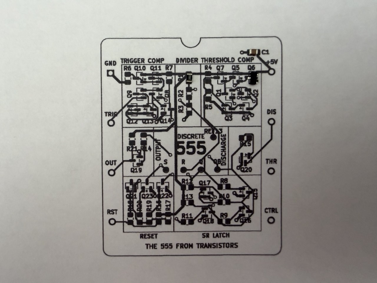
The files are correct. A last check needs no software: the board at its true size, with the parts on it. No program knows the size of the part in your hand. A footprint at the wrong pitch, or for the wrong package, passes each check before this one.
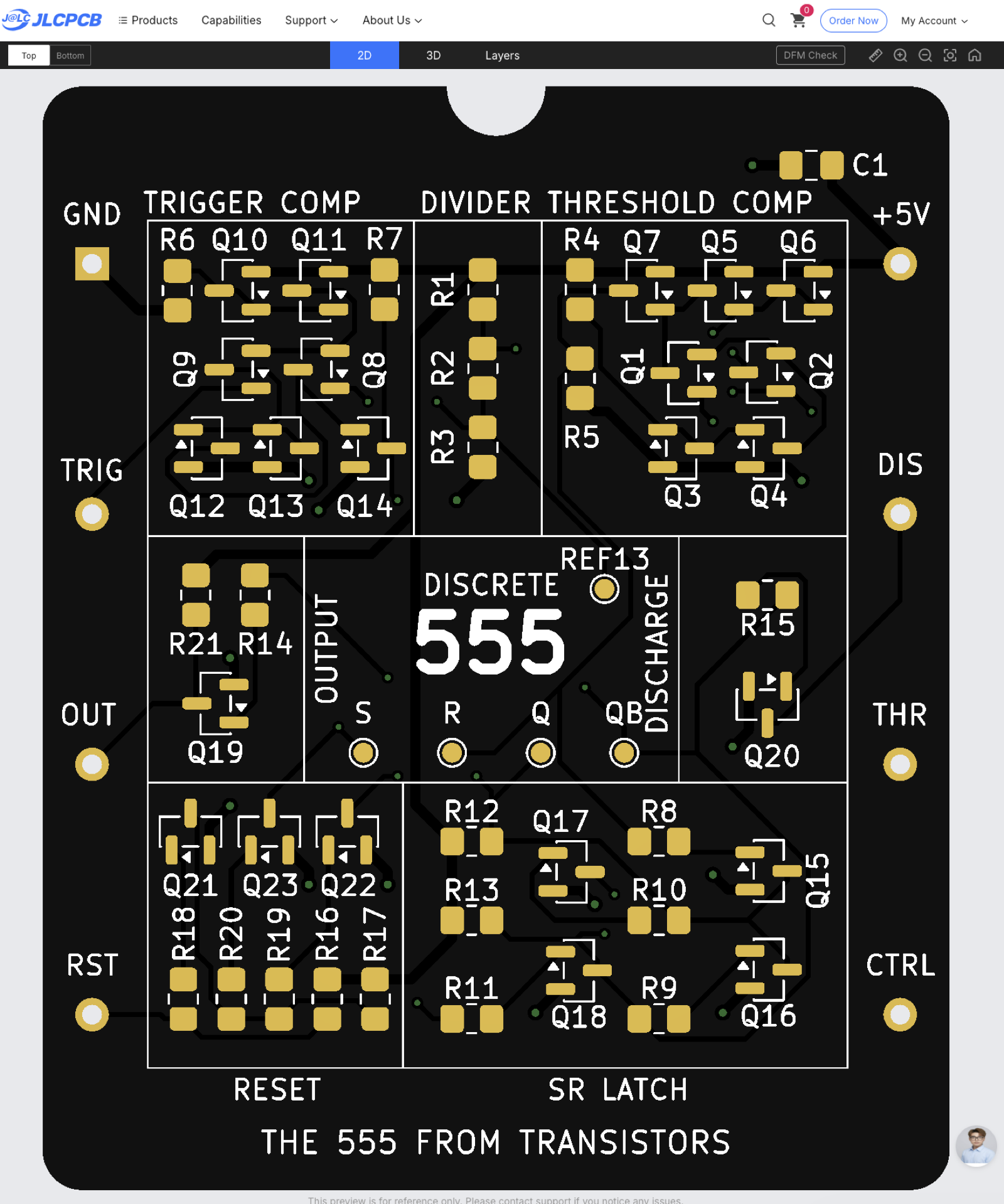
The board passed each check on this side. Now the board house checks the files against what its machines can make. Upload the ZIP on the order page of the board house. The board house reads the size of the board from the outline and shows the board in its own viewer. Figure 19-2 is that viewer for the files of this course. Each layer, each label and the notch are there, so they are in the files.
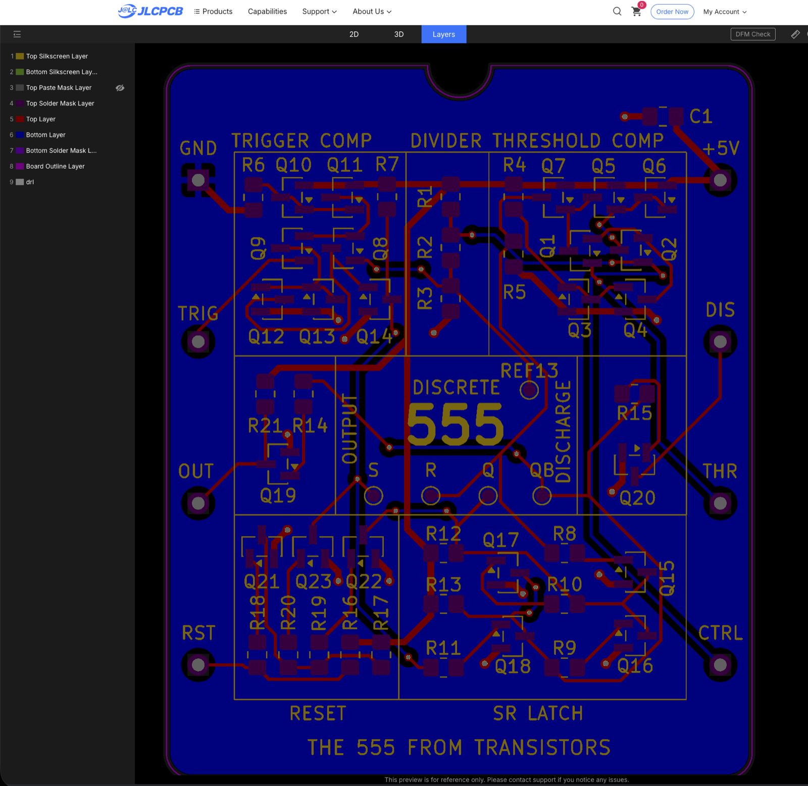
The board house also checks its own limits: the narrowest track, the smallest gap, the smallest hole and the distance from copper to the edge. Compare them with the values of the board before you upload. Board Statistics gives them: on this board, tracks of 0.254 mm or wider, gaps of 0.2032 mm or wider and holes of 0.3048 mm or larger. Experiment 18 took the copper-to-edge clearance of 0.3 mm and the text height of 1.0 mm from the limits of JLCPCB in July 2026. The limits differ between board houses and can change, so read the limits of your board house when you order.
The order form has a few fields that matter. The table gives the values for the board of this course, which was ordered from JLCPCB on 8 July 2026. The names of the fields differ between board houses.
| Field | Value | Reason |
|---|---|---|
| Layers | 2 | F.Cu and B.Cu |
| Dimensions | 46 × 56 mm | Read from the outline |
| Thickness | 1.6 mm | The stackup of Board Setup |
| Outer copper | 1 oz | 0.035 mm, the copper of the stackup |
| Surface finish | Lead-free HASL | Solder over the copper of each pad, without lead |
| Colour of the mask | Black | A choice of appearance only |
| Quantity | 5 | Spare boards for a second build or an error in assembly |
Keep the other fields at their default values. Experiment 20 solders each part with an iron, so the order needs no stencil. A stencil is a metal sheet with an opening for each pad. It is for solder paste and a hot plate, and the board house cuts it from the paste layers. If you want to use paste, order the stencil with the boards.
The files of an order are correct for one version of the board only. If you move a track or a label after the export, the ZIP describes a board that no longer exists. After each change, write the files again, do the checks of this experiment again, and give the new ZIP a new version.
Now place the order. Submit the order form and pay for it. Keep the uploaded ZIP with the project, and record the order number. If a board does not agree with the design later, that ZIP shows the files that the factory used.
Three questions on this experiment. They ask why the files need a separate viewer, what a check that cannot run reports, and what the paper test finds.
1. Why check the Gerber files in GerbView as well as in the PCB Editor?
The PCB Editor shows the board file. The factory makes the board from the exported files. A layer that is missing from the export, or an outline that was not plotted, shows only in a viewer that reads the exported files.
2. The parity check runs on a copy of the board with a different name. What does its report give?
kicad-cli finds the schematic by the name of the board file. On a copy with another name it writes a message to the terminal, and the report gives 0. A check gives a zero that means something only if it can also fail.
3. A footprint has the wrong pitch for its part. Which check finds it?
The design rules checker and the parity check compare the board with rules and with the schematic. Neither knows the size of the part in your hand. Only the part on its printed pads shows that the pitch is wrong.
The board passed each check. The design rules checker is at 0, and the pins are in the order of the NE555. The files are 12, with 39 holes. In the paper test each part covers its pads, and the viewer of the board house shows the complete board. The order is placed, with the ZIP of its files kept with the project. That is the second milestone of the course: the design of the board is complete. The factory makes the board, and the wait for it takes some days to some weeks. Experiment 20: Assembly Day solders the 46 parts on the board when it arrives.