Full Stack Electronics · Stage Four · Experiment 20
The seventh step from the breadboard to a printed circuit board. Sort the 45 surface-mount parts by their markings, solder them by hand block by block, add the eight pins, and inspect each joint before the first power-up.
Experiment 19 ended with the order. The boards of this course came back from JLCPCB six days later: five black boards with lead-free HASL, and no parts on them. This experiment puts the parts on one board. There are 46: 23 transistors, 21 resistors and C1, which are surface-mount parts, and the eight pins of J1. The parts are small. An 0805 is 2.0 mm long, and a SOT-23 is 2.9 mm long. The NPN and the PNP transistors have the same package and the same footprint, and only a code on the top tells them apart. A PNP in an NPN position gives a joint that looks correct and a board that does not work. So this experiment sorts the parts first, solders them block by block, and inspects each joint under magnification. The result is a board that is ready for its first power-up in Experiment 21.
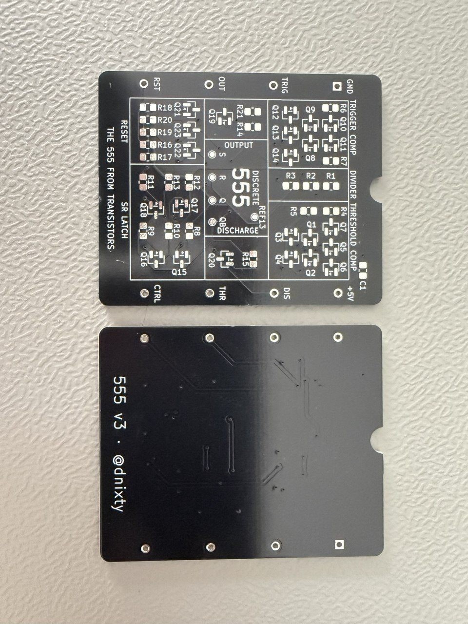
Figure 20-1 shows the bare board. The table gives the parts that go on it, with the code that each part carries and its designators on the silkscreen.
| Quantity | Part | Code on the part | Designators |
|---|---|---|---|
| 16 | NPN transistor, MMBT3904, SOT-23 | 1AM | Q1 to Q4, Q12 to Q23 |
| 7 | PNP transistor, MMBT3906, SOT-23 | 2A | Q5 to Q11 |
| 8 | 4.7 kΩ resistor, 0805 | often 4701 | R1 to R7, R21 |
| 10 | 10 kΩ resistor, 0805 | often 1002 | R8 to R11, R14, R15, R17 to R20 |
| 2 | 1 kΩ resistor, 0805 | often 1001 | R12, R13 |
| 1 | 100 kΩ resistor, 0805 | often 1003 | R16 |
| 1 | 0.1 µF capacitor, 0805 | None | C1 |
| 1 | 1×8 pin header, cut into eight single pins | None | J1 |
Many 1 % resistors carry a code of four digits: three digits of value and the number of zeros after them. So 4701 is 470 with one zero, 4.7 kΩ, and 1002 is 100 with two zeros, 10 kΩ. Some resistors carry no code at all. Keep each value in its own place from its packet to the board, because you cannot read the value of a resistor without a code. Ceramic capacitors of this size usually carry no code. The five test pads, TP1 to TP5, get no part. They stay bare copper for the probe of Experiment 21.
Of all the parts in the table, the transistors need the most care. Figure 20-2 shows why: the NPN and the PNP are the same package, with the same three legs in the same places.
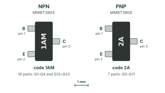
Once a transistor is soldered, flux often covers its code, and a wrong transistor looks the same as a correct one. A wrong transistor gives no short and no bad joint. It gives a board that does not work, with no visible fault. So sort the transistors before you switch on the iron.
1AM on NPN, 7 with 2A on PNP.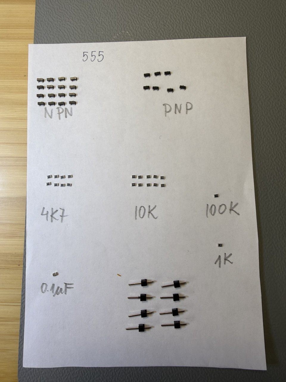
The parts are sorted. Before the first joint, set up the bench for small parts.
With the bench ready, solder one block at a time, in the boxes of the silkscreen. Start with the divider, then the two comparators and the latch, then the output and discharge transistors, and the reset block last. In each block, solder the resistors first and then the transistors. A board that you stop on halfway then shows which block comes next. The board of this course was soldered by hand with an iron, each joint in turn. Figure 20-4 shows the four steps for an 0805.
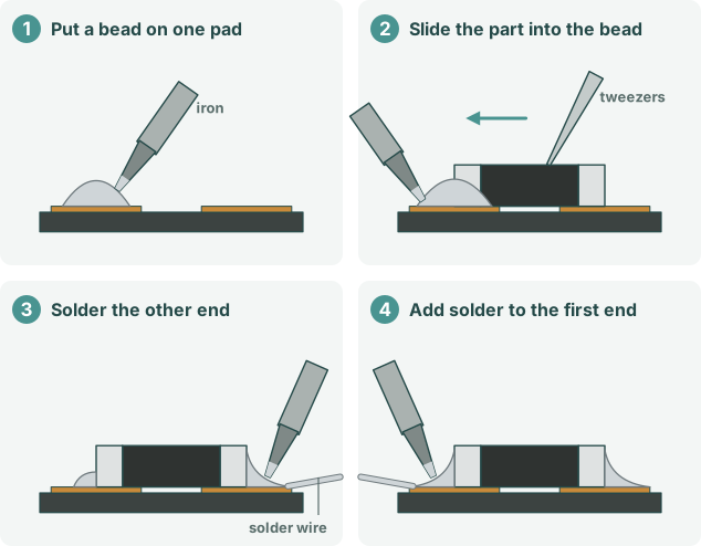
1AM for Q1 to Q4 and Q12 to Q23, 2A for Q5 to Q11. Put a bead on the pad of pin 3, the leg that is alone on its side, and solder that leg as in step 2. Check that the part lies flat on all three pads. Then solder pins 1 and 2.A SOT-23 has two legs on one side and one on the other, so it fits its footprint in one way only. The kind of transistor is the only thing that can be wrong, and the code check at each transistor finds it.
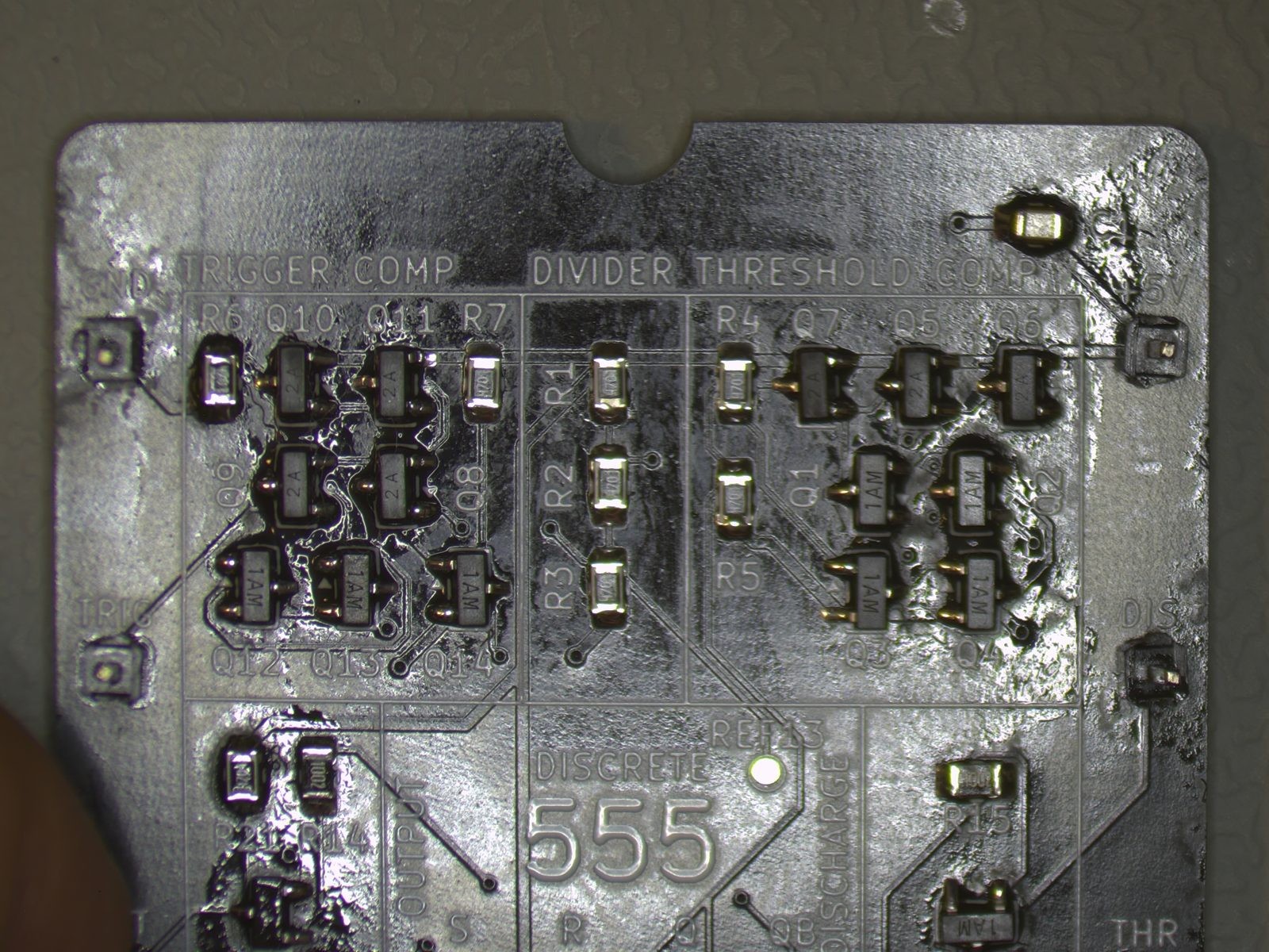
1AM on the NPN transistors and 2A on the PNP transistors. The gloss is flux. Click to enlarge.The surface-mount parts are on the board. The pins of J1 go on last. They are the only through-hole joints, and they need more heat than the small parts. Until they are on, the board lies flat under the microscope, and nothing tall can catch a sleeve.
The pins point up from the front, so the socket of a jumper lead goes onto each pin from above. In Experiment 21, eight jumper leads connect each pin to the row of the breadboard where the same pin of the NE555 sat in Experiment 1.
All the parts are now on the board. Before any voltage, inspect the board under the microscope, one joint at a time. A fault that you find now costs a minute with the iron. In Experiment 21, the same fault can stop the timer or trip the current limit of the supply. Then you must find it on a board with voltage on it. Figure 20-6 shows the four things to look for at each joint.
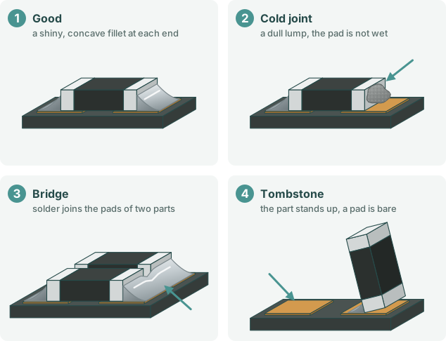
| Fault | What you see | Correction |
|---|---|---|
| Cold joint | A dull lump of solder that does not flow onto the pad | Apply flux and melt the joint again until the solder flows into a fillet |
| Bridge | Solder that joins two pads or two legs | Put solder wick on the bridge and press it with the iron. The wick takes up the solder. |
| Tombstone | An 0805 that stands on one end, with the other end up | Melt the end that is down, push the part flat, and solder the other end |
| Wrong transistor | 2A where 1AM must be, or the opposite | Read each code one last time against the table. Remove a wrong part with the iron and solder the correct part. |
Under the microscope, the board looks glossy, because the no-clean flux stays on it. Figure 20-7 shows this. The residue does no electrical harm. Isopropyl alcohol and a soft brush remove it, after the first power-up. Do not let the gloss hide a joint: if you cannot see a joint clearly, melt it again.
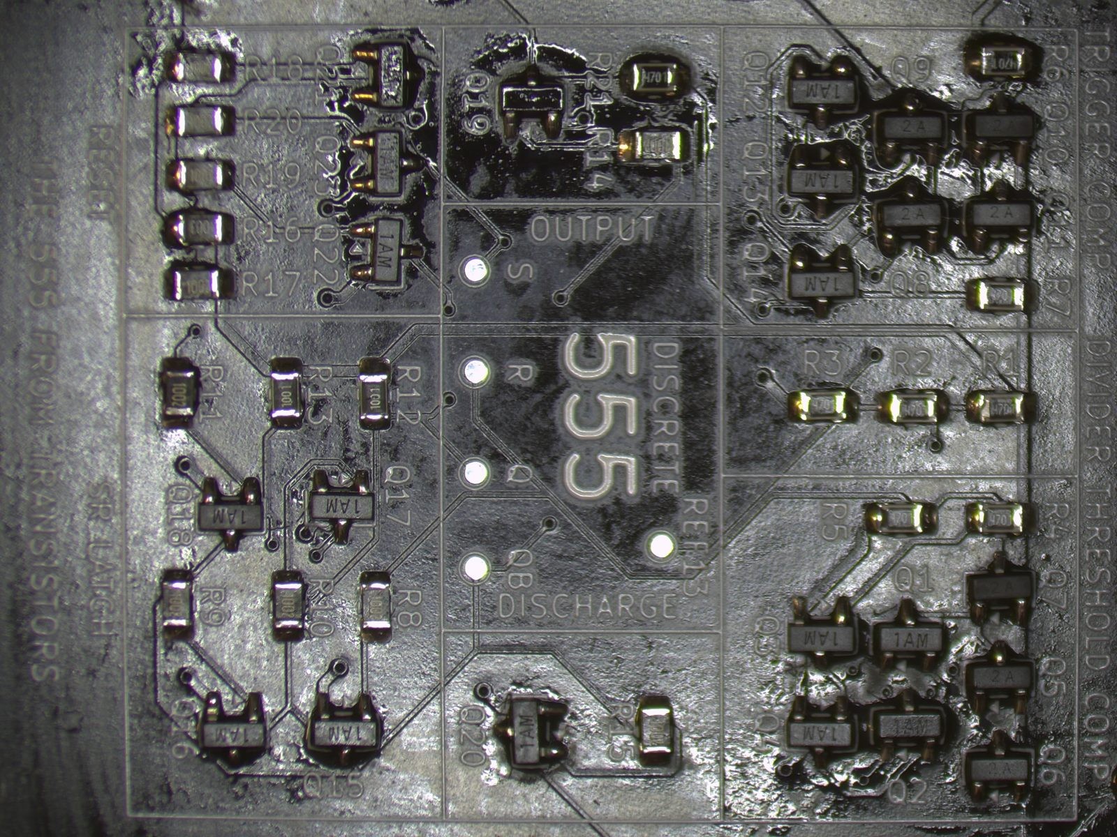
The tip of the iron is hot enough to burn skin and to start a fire in paper. Put the iron in its stand after each joint. Keep isopropyl alcohol, paper and batteries away from the iron. Use the fume extractor, and do not breathe the smoke of the flux.
A hot plate can solder all the surface-mount parts at once. You put a small amount of solder paste on each pad, from a syringe or through a stencil, and put each part on its pads. Then the board goes on a hot plate at the temperature that the paste needs. When the paste melts, the liquid solder pulls each part to the middle of its pads. Read each code before you put the transistor on the paste, as for the iron. The pins of J1 still go on last, with the iron. The board of this course was soldered with the iron only.
Three questions on this experiment. They ask how to tell the transistors apart, why the pins go on last, and what a good joint looks like.
1. What tells an MMBT3904 from an MMBT3906 on this board?
The two have the same SOT-23 package and the same footprint. Only the code on the top is different, so sort them by the code before you solder, and read the code again at each position.
2. Why do the eight pins go on after the surface-mount parts?
A through-hole pin needs more heat than an 0805. A board with no tall parts lies flat under the microscope, and nothing on it can catch a sleeve.
3. How does a good joint of an 0805 look under the microscope?
Solder that wets flows onto the pad and the end cap, and makes a concave fillet. A dull lump that does not reach the pad is a cold joint. Solder across two pads is a bridge.
The board has its 45 surface-mount parts and its eight pins. Each joint is a fillet, with no bridge, no tombstone and no wrong transistor. That is the seventh step from the breadboard to the board. The board has had no voltage yet. Experiment 21: First Power-Up applies the first voltage, with a current limit, and puts the board in place of the NE555.