Full Stack Electronics · Stage Three · Experiment 13
Add three transistors for pin 4 of the NE555. A low on RESET stops the timer and empties the capacitor, and the next cycle starts from 0 V.
Experiment 12 closed the loop, and the board runs as a 555 astable. Nothing outside the board can stop it. The NE555 has one more input for that: pin 4, RESET. In Experiment 1, pin 4 went to +5 V, so the reset stayed off. The TI datasheet for the NE555 gives the rule in its function table. While RESET is low, the output is low and the discharge transistor is on. TRIGGER and THRESHOLD then have no effect. The datasheet also says that RESET is used to start a new timing cycle.
On this board a low on RESET must do two things. It must hold Q at 0, so that Q19 turns the LED off. It must also hold DIS at 0 V, so that C empties. This experiment adds the reset block, three transistors Q21 to Q23, and a fifth lead for the 555's pins, RESET. Q21 and Q22 go in first, and the oscilloscope shows what they do not do. Q23 then completes the reset.
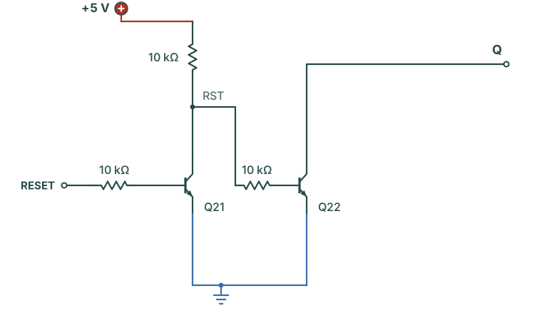
RESET is active low: it acts when it is 0. A transistor switch acts when its base gets a 1. So the reset block starts with an inverter, Q21, the transistor switch of Experiment 3. Figure 13-1 shows Q21 and the first transistor that it drives, Q22.
Q22 is a third transistor on Gate 1's pull-up. Gate 1 is now a NOR gate with three inputs: R, Q̄ and RST. A 1 on any input makes Q 0, as in the NOR gate of Experiment 10.
Q22 must hold Q at 0 against Gate 1's 1 kΩ pull-up.
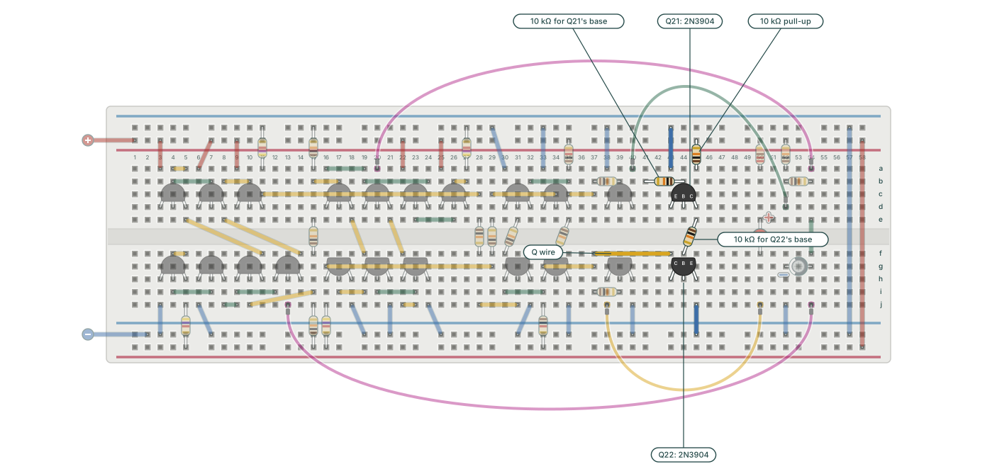
Q21 and Q22 are inside a 555, so they go next to Q19 and Q20. Experiment 12 left columns 41 to 49 free for them, between Q19 and the LED. Q21 and Q22 stand one above the other in columns 43 to 45, two columns right of Q19 and Q20, as Q19 and Q20 stand two columns right of the latch. Q21 faces the same way as Q20, and Q22 the same way as Q19. Q21's base resistor runs back into the two columns between, to column 41. A resistor needs its legs at least three columns apart, because its body is longer than two hole spacings. A 10 kΩ diagonally across the centre channel takes RST from Q21's collector to Q22's base, and a wire along row f takes Q to Q22's collector. Figure 13-2 shows the new parts.
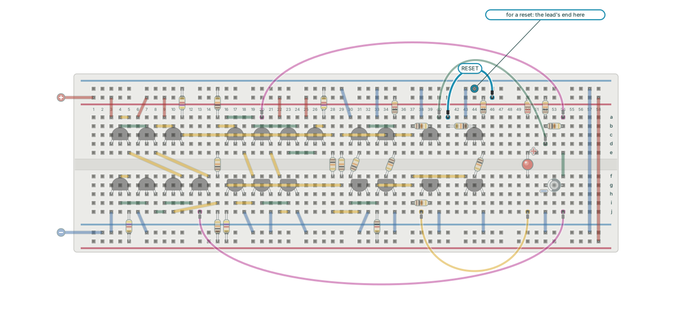
RESET is a pin of the 555, so a lead connects it to the outside, as for OUT, DIS, TRG and THR. In Experiment 1, pin 4 went to +5 V. The RESET lead does the same here. For a reset, its end moves to the ground rail next to it. Figure 13-3 shows both positions.
If the LED stays dark, RST is not near 0 V and Q22 holds Q at 0. Switch off, and check that the RESET lead is in the +5 V rail. Then check Q21, its emitter jumper and its base resistor.
Keep the lead's end in a rail. With the end loose, no current flows into Q21's base. Q21 is then off, and the board stays in reset. A loose lead can also pick up noise. The NE555 datasheet gives the same rule: to prevent false triggering, connect RESET to VCC when it is not used.
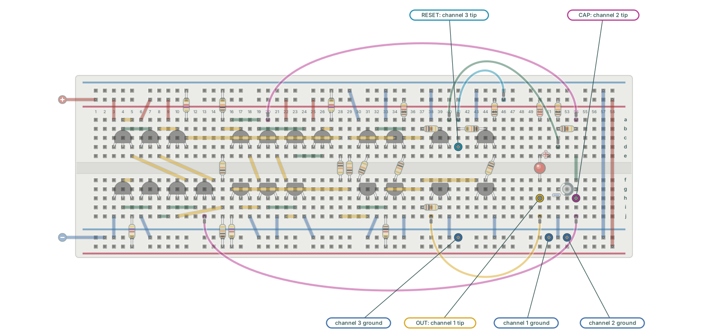
A reset happens between two moves of the lead, so the oscilloscope must catch it on one sweep. Channel 3 shows RESET and triggers the sweep when RESET rises again. Channels 1 and 2 stay on OUT and CAP, as in Experiment 12.
| Oscilloscope channel | Tip or hook | Ground clip |
|---|---|---|
| Channel 1: OUT | 50h, the LED's cathode | Inner bottom rail, column 51 |
| Channel 2: CAP | 54h, C's positive lead | Inner bottom rail, column 53 |
| Channel 3: RESET | 41d, the strip of the RESET lead | Inner bottom rail, column 41 |
While RESET is low, OUT is high and the LED is dark. That part works. Now look at CAP. At the start of the reset it falls, as in a normal discharge. Then it stops at the lower turning point and stays there until RESET rises. In Figure 13-5 the reset lasted longer than the left half of the screen, so CAP is already flat at the left edge, at 1.68 V. After the release the LED lights, and the first charge starts from that level and ends at the upper turning point, 3.30 V.
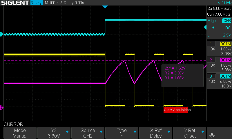
The datasheet asks for the discharge transistor on during a reset. On the board, C stops near 1/3 of the supply, so Q20 does not stay on. Q22 holds Q at 0, but Gate 2 still has its other input, S. With Q at 0, Gate 2 is an inverter for S, and the trigger comparator continues its work. Follow Figure 13-6 through the loop that remains.
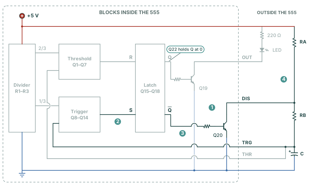
Q20 discharges C only while CAP is above 1/3. So CAP stays near the lower turning point for as long as RESET is low. After the release, the first charge starts from that level, as every charge does. The timer continues as if the reset had not happened, and the datasheet's new timing cycle does not start.
Q20 takes its signal from the latch, and S can change the latch during a reset. So the reset needs a transistor on DIS that the latch does not control. Q23 is that transistor. Its collector goes to DIS, beside Q20's collector, and its base takes RST, as Q22's base does. Figure 13-7 adds it.
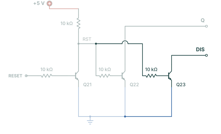
During the reset both latch outputs are 0: Q22 holds Q, and S holds Q̄. Experiment 11 found the same state with S and R both at 1, and here RST takes the place of R. It does no harm, because Q19 and Q20 are both off and Q23 alone holds DIS. Experiment 11 also found that the next state depends on the input that returns to 0 last. When RESET rises, RST returns to 0 and S is still 1, so S sets the latch. Q rises, the LED lights, and C charges from 0 V.
RST now drives two bases. The pull-up and the two 10 kΩ base resistors give (5 V − 0.7 V) / 15 kΩ = 0.29 mA, so each base gets 0.14 mA. Q22's 5 mA then needs a current gain of about 35, still far below 100. Q23 takes RA's 0.5 mA and the current from C, less than 1 mA in total.
Q23 goes in the upper block, in columns 47 to 49, and faces the same way as Q20 and Q21. Its base resistor runs along row b from the upper strip of column 45, RST. A yellow wire along row e joins its collector to DIS. Figure 13-8 shows the new parts.
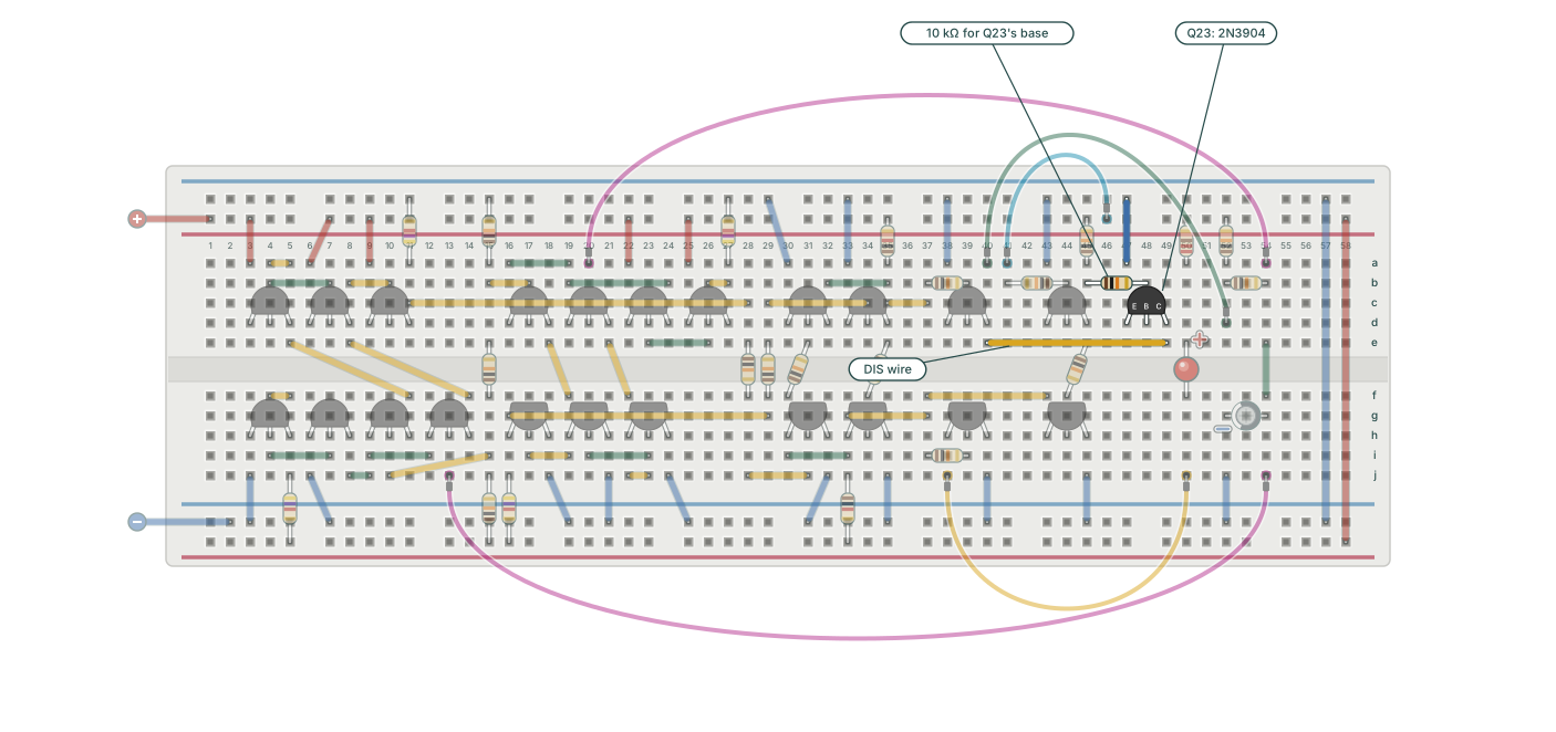
Keep the oscilloscope as it is. Switch on the 5 V supply, and reset the timer as before: the lead's end in the outer top rail at column 44 for about half a second, then back in the inner rail.
While RESET is low, OUT is high and the LED is dark, as before. CAP now falls past the lower turning point and continues down to near 0 V. After the release the LED lights at once, because CAP is below 1/3 and S sets the latch. The first charge then starts from near 0 V, so the LED stays on for longer than in each later cycle. By calculation the first charge takes about 220 ms, and each later charge 139 ms. The box “Where the 220 ms comes from” calculates the first one. In Figure 13-9 the cursors measure the first charge, from the release to the first rise of OUT: 210 ms. Each later charge is about 1.3 divisions, 130 ms, as in Experiment 12. The ratio of the two is 1.6 on the board and 220 ms / 139 ms = 1.6 by calculation.
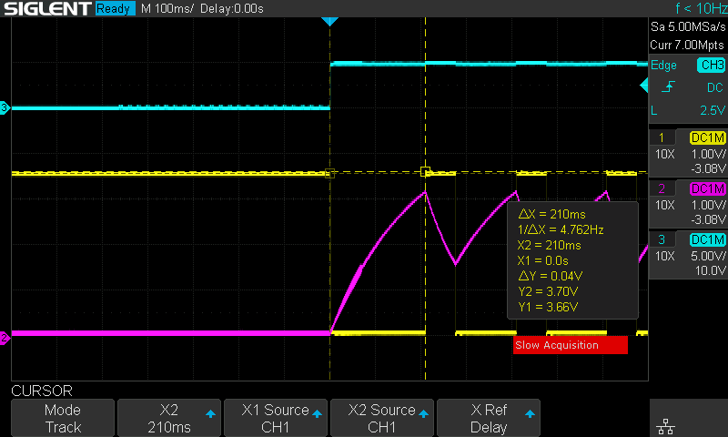
If CAP still stops near the lower turning point, Q23 does not hold DIS. Switch off, and check Q23, its emitter jumper, its base resistor and the DIS wire along row e. If CAP stays near 0 V after the release, RST did not fall again: check that the RESET lead is back in the +5 V rail.
During a charge CAP moves towards 5 V through RA + RB, and the gap between the supply and CAP gets smaller. A normal charge starts with a gap of 2/3 of the supply and ends with a gap of 1/3, so the gap halves. That takes 0.69 RC, as Experiment 12 calculated: 139 ms.
The first charge after a reset starts with CAP at 0 V, so the gap is the full supply. It ends at the upper turning point, where the gap is 1/3 of the supply. So the gap falls to one third. That takes 1.10 RC: 1.10 × 20 kΩ × 10 µF = 220 ms. The first LED-on time is about 1.6 times as long as the others.
Call the supply . During a charge from 0 V, the gap falls as
The charge ends when the gap is one third of the supply:
Divide both sides by :
Take the natural logarithm of both sides. The logarithm of one third is minus the logarithm of 3:
Multiply both sides by :
With and , , so .
The reset on this board has two jobs, and each job has its own transistor. Q22 holds Q at 0, so the output is low. Q23 holds DIS near 0 V, so C empties. Q21 inverts RESET for both of them. The table compares the board with the function table of the NE555 datasheet.
| While RESET is low | NE555 datasheet | Q21 and Q22 | Q21 to Q23 |
|---|---|---|---|
| Output | Low | OUT high, LED dark | OUT high, LED dark |
| Discharge | On | Q20 on only above 1/3 | Q23 on |
| Capacitor | Discharges | Stays near 1/3 | Falls to near 0 V |
| First charge after the release | A new timing cycle | The normal length | About 220 ms |
The output on this board is the opposite way up from pin 3, as Experiment 12 explained, so the LED is the output to compare. The first attempt held the output, and the discharge still followed the latch. S changes the latch, and the trigger comparator sets S whenever CAP is below 1/3, during a reset too. A reset that acts only on the latch shares the latch with S. Q23 acts on DIS directly, after the latch, so no signal from the comparators reaches it. That is how RESET overrides the other inputs, as the datasheet says.
A square wave on RESET turns the timer on and off. Set channel 1 of the function generator to a square wave at 1 Hz, low level 0 V and high level 5 V, with the load set to HiZ (Experiment 3 explains why). Take the RESET lead's end out of the rail, clip the generator's red lead on it, and clip the black lead to the inner bottom rail. Then switch on the output. The LED blinks for half a second and stays dark for half a second, and each burst starts with the long first charge. When you finish, switch off the output and put the lead's end back in the +5 V rail.
Three questions on this experiment. They ask why the timer runs with RESET high, why two transistors were not enough, and why the first charge after a reset is longer.
1. The RESET lead is in the +5 V rail, and the timer runs because…
Current through Q21's 10 kΩ turns it on, and it holds RST near 0 V. Q22 and Q23 then get no base current, so the latch and Q20 work as in Experiment 12.
2. With only Q21 and Q22, CAP stops near 1/3 during a reset, because…
Q22 holds only Q. Gate 2 still takes S, and the trigger comparator sets S whenever CAP is below 1/3. So Q20 turns off at 1/3 and C charges again. Q23 holds DIS without the latch.
3. After a full reset, the first LED-on time is about 220 ms instead of 139 ms, because…
A normal charge halves the gap between the supply and CAP, which takes 0.69 RC. From 0 V the gap falls to one third, which takes 1.10 RC.
This is the last experiment of Stage Three, and the breadboard prototype is complete. The board now has all eight pins of the NE555: the two rails for pins 8 and 1, the five leads for pins 2, 3, 4, 6 and 7, and the divider's 2/3 tap for pin 5, CONTROL. Twenty-three transistors do the work of the chip, and each block was tested on the bench before the next one went in. Stage Four puts the same circuit on a printed circuit board. Experiment 14: The Master Schematic draws the whole circuit as one schematic, with a designator for each part.