Full Stack Electronics · Stage Three · Experiment 12
Add two transistors and the timing parts of Experiment 1, connect the blocks in a loop, and take the generator away. The board then runs as a 555.
Experiment 11 finished the last block of the timer. The board now holds both comparators, the divider that sets their references, and the latch. Nothing connects them yet. In Experiment 9 the function generator made the ramp for the comparators, and in Experiment 11 it set and reset the latch. A timer must make its own ramp and its own S and R pulses.
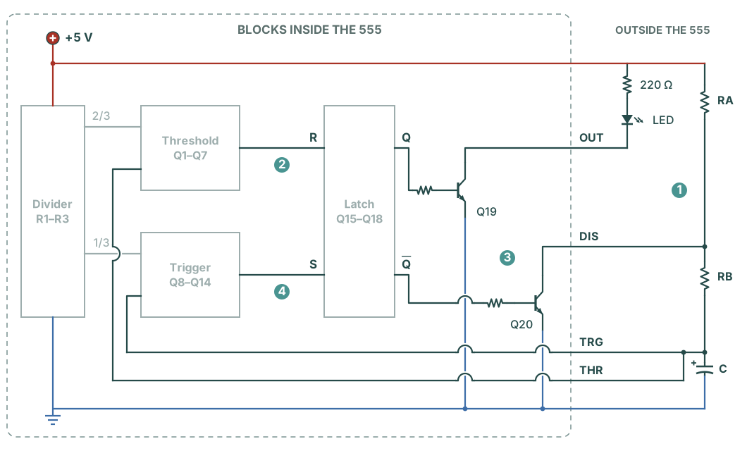
The NE555 of Experiment 1 does this with a capacitor and two resistors outside the chip, and two transistors inside it. One transistor empties the capacitor, and the other drives the load. This experiment adds those two transistors, Q19 and Q20, and the resistors and the capacitor of Experiment 1. Then it connects the blocks in a loop, and the capacitor takes the generator's place. That change is the swap. The last section measures the board in the same way as the NE555 in Experiment 1. Figure 12-1 shows the loop. The parts in the dashed outline are the parts inside a 555. The pale boxes are the blocks that are already on the board.
Experiment 11 drove S and R from the generator. In the loop, the two comparators drive S and R, and the capacitor voltage drives both comparators. Call that voltage CAP. Follow Figure 12-1 through one cycle:
Each comparator's OUT is 1 only for a short time near its level. For the rest of the cycle both are 0, and the latch alone keeps the timer charging or discharging. Those are the two hold states of Experiment 11. C charges through RA and RB in series and discharges through RB alone. So the charge takes about twice as long as the discharge, and the LED is lit for about two-thirds of each cycle, as on the NE555.
The loop needs two parts that the board does not have yet: Q19 and Q20. Figure 12-2 shows them with the timing parts. Each one is the transistor switch of Experiment 3, with a 10 kΩ into its base, its emitter at ground and its load on its collector.
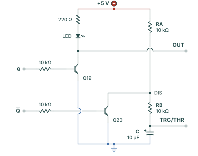
Q20 is the discharge transistor. In the NE555 it is the transistor on pin 7, DISCHARGE. Its collector goes to DIS. When Q̄ is 1, Q20 turns on and holds DIS near 0 V, so C discharges through RB. When Q̄ is 0, Q20 is off, and the current through RA continues through RB into C. Without Q20, nothing discharges C. It charges past 2/3 towards 5 V, R stays at 1, and the timer stops after the first charge.
Q19 is the output buffer. A buffer is a stage that drives a load, so that the circuit before it supplies only a small current. The LED and its 220 Ω hang from the +5 V line to Q19's collector. When Q is 1, Q19 turns on and the LED lights. By calculation the LED then takes about 13 mA, and Q supplies only Q19's base current.
Why not connect the LED to Q directly? A 1 on Q comes through Gate 1's 1 kΩ pull-up. With the LED and its 220 Ω on Q, the current comes through that 1 kΩ. By calculation the LED then takes about 2.5 mA, and the 1 on Q falls to about 2.5 V. In Experiment 2 the LED did the same to the CD4001B's Q: its 1 fell to about 2.6 V. The NE555 has a separate output stage after its latch for the same reason.
The LED lights while C charges, as on the NE555 in Experiment 1. The voltage at Q19's collector is the opposite way up from pin 3 of the NE555, because Q19 inverts. Call that collector OUT. OUT is near 0 V while C charges and high while C discharges. The board of Stage Four takes Q19's base from Q̄ instead, so that its OUT matches pin 3. On the breadboard the LED is the output, and it matches.
Experiment 11 found that a 1 on Q or Q̄ is about 4.6 V, because the output also drives a base through a 10 kΩ. Now Q drives the bases of Q17 and Q19, and Q̄ drives the bases of Q16 and Q20.
4.3 V is still far above the 1.10 V where a transistor switch from Experiment 3 finishes its change. The 0.36 mA is also enough for each new transistor. The onsemi datasheet for the 2N3904 gives a current gain of at least 100 at 10 mA, so Q19's 13 mA needs about 0.13 mA of base current. Q20 carries less than 1 mA. Experiment 11 warned that each extra base lowers the 1 again. With two bases on each output, the 1 stays near 4.3 V.
Figure 12-2 gave the circuit. On the board, the new parts go in two groups, as in Figure 12-1. Q19 and Q20 are inside a 555, so they go next to the latch. The LED, its 220 Ω, RA, RB and C are outside a 555, so they go further right. Wires on the board connect the blocks inside the 555, as in Experiment 2. Four jumper leads then connect the 555's pins to the parts outside it.
The wires need room. The latch moves two columns right, so columns 28 and 29 become free for the R and S resistors. The rail links in columns 38 and 39 move to columns 57 and 58, so that they stay at the right end of the circuit. The drawings now show 58 of the board's 63 columns. Figure 12-3 shows the board after these moves.
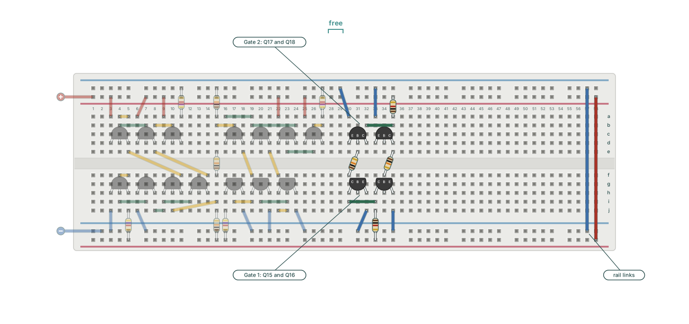
Move one part at a time, and check its new holes against Figure 12-3 before you move the next part.
Move each part to the right. A pull-up moved two columns left goes into a base strip. On my board Gate 2's pull-up went into 31a, Q17's base. Q17 then stayed on and held Q̄ at 0, so Q20 did not discharge C. At switch-on the LED flashed once and then stayed dark.
The latch now ends at column 35. Q19 and Q20 go two columns to its right, in columns 38 to 40, Q19 in the lower block and Q20 in the upper block. Their base resistors lie along a row, so that the wires from the latch can reach them along a row too. The parts outside the 555 go in columns 50 to 54, and columns 41 to 49 stay empty between the two groups. Experiment 13 adds the last block inside the 555 in those columns, so no part outside the 555 has to move again. Figure 12-4 shows the new parts.
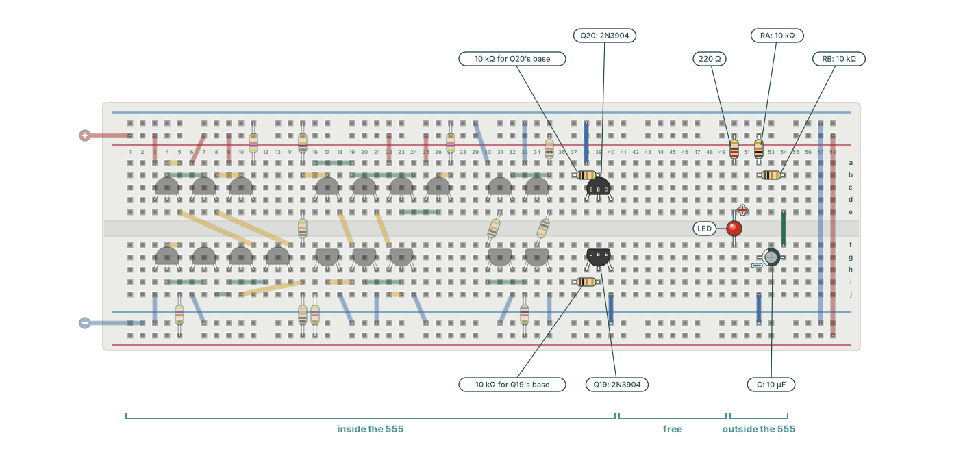
Check the polarity of C before you apply power. The stripe on the electrolytic marks its negative lead, and that lead goes into the ground rail. A reversed electrolytic can become hot or vent.
Experiment 1 called the timing resistors R1 and R2. On this board R1 to R3 are the divider of Experiment 9, so the timing resistors take the names from the NE555 datasheet: RA and RB.
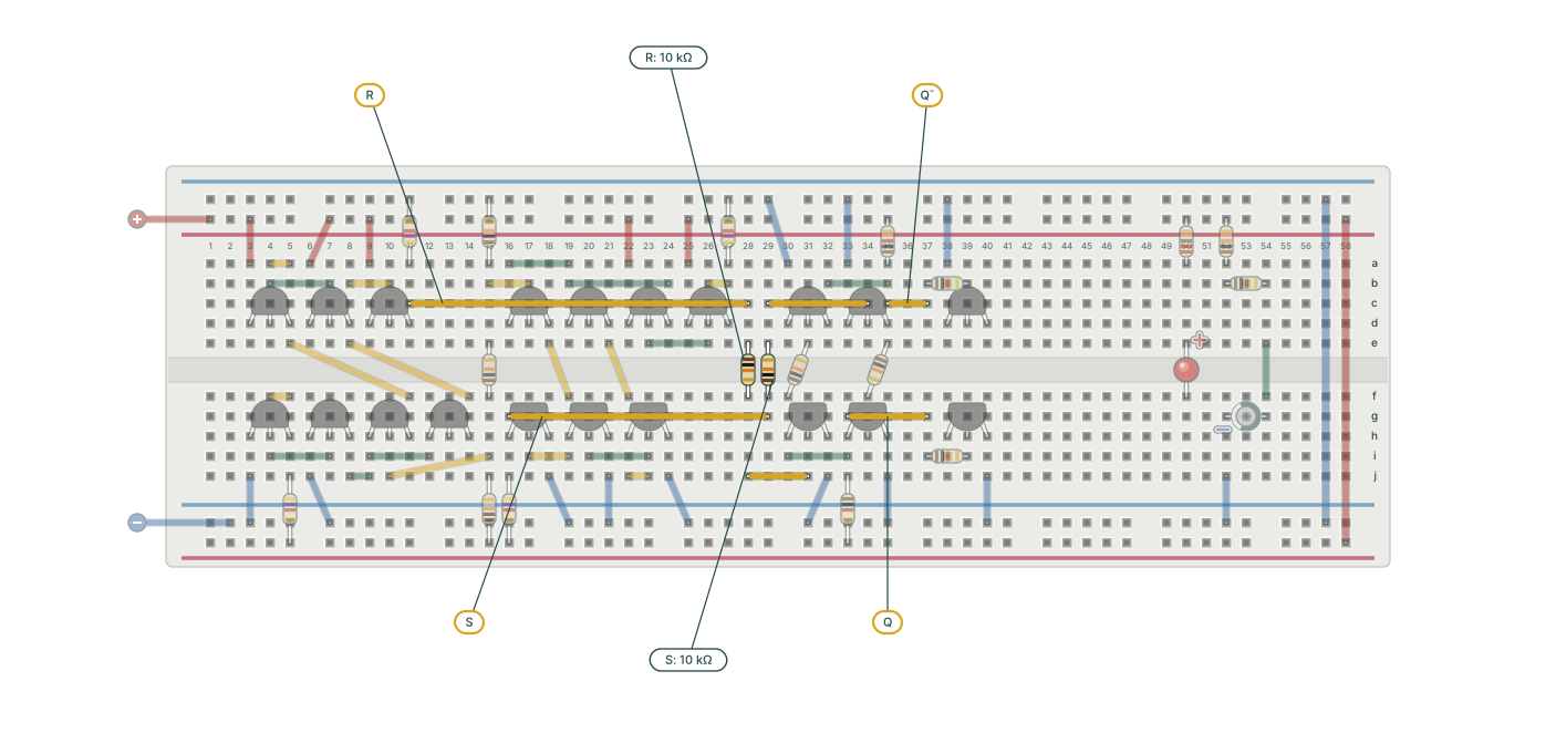
The new parts are in place, and the blocks are still separate. First, wires on the board connect the blocks inside the 555: S and R from the comparators to the latch, and Q and Q̄ from the latch to Q19 and Q20. Rows c and g have no parts in them, because the transistor legs are in rows d and h. So the wires lie along those rows, under the transistor bodies. The 10 kΩ resistors of R and S cross the centre channel in the free columns 28 and 29, from the comparator's block to the latch gate in the other block. Figure 12-5 shows the wires.
The blocks inside the 555 are now connected. A 555 connects to the parts outside it through its pins. Four jumper leads do the same here, and Figure 12-6 tags each one with the pin name:
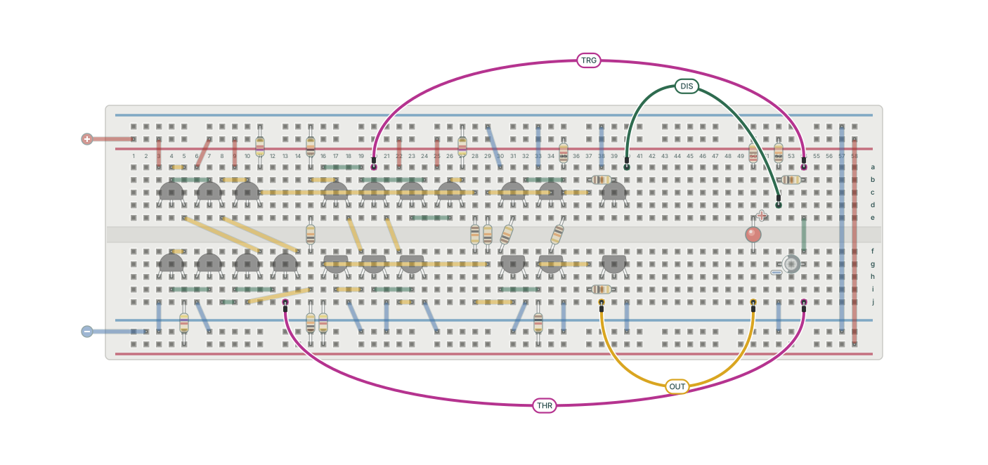
The routes in Figure 12-6 keep the leads apart and clear of the parts. A different route works too, if each lead's two ends go into the correct holes.
All the connections of Figure 12-1 are now on the board. Set the 5 V supply to 5.00 V with a 50 mA current limit, and switch it on. Expect the LED to blink about five times a second and to stay on about twice as long as it stays off.
The LED lights as soon as the supply is on. At that moment C is empty and CAP is 0 V. That is below 1/3 of the supply, so the trigger comparator's OUT is 1 and S sets the latch. Q rises, the LED lights, Q20 stays off and C starts to charge. An empty capacitor is the condition that the trigger comparator detects, so the timer starts by itself.
Switch the supply off before you change anything. Then work through these checks:
The board blinks at about the NE555's rate. The oscilloscope shows how close it is. Use the method of Experiment 1: channel 1 on the output, channel 2 on the capacitor.
| Oscilloscope channel | Tip or hook | Ground clip |
|---|---|---|
| Channel 1: OUT | 50h, the LED's cathode | Inner bottom rail, column 51 |
| Channel 2: CAP | 54h, C's positive lead | Inner bottom rail, column 53 |
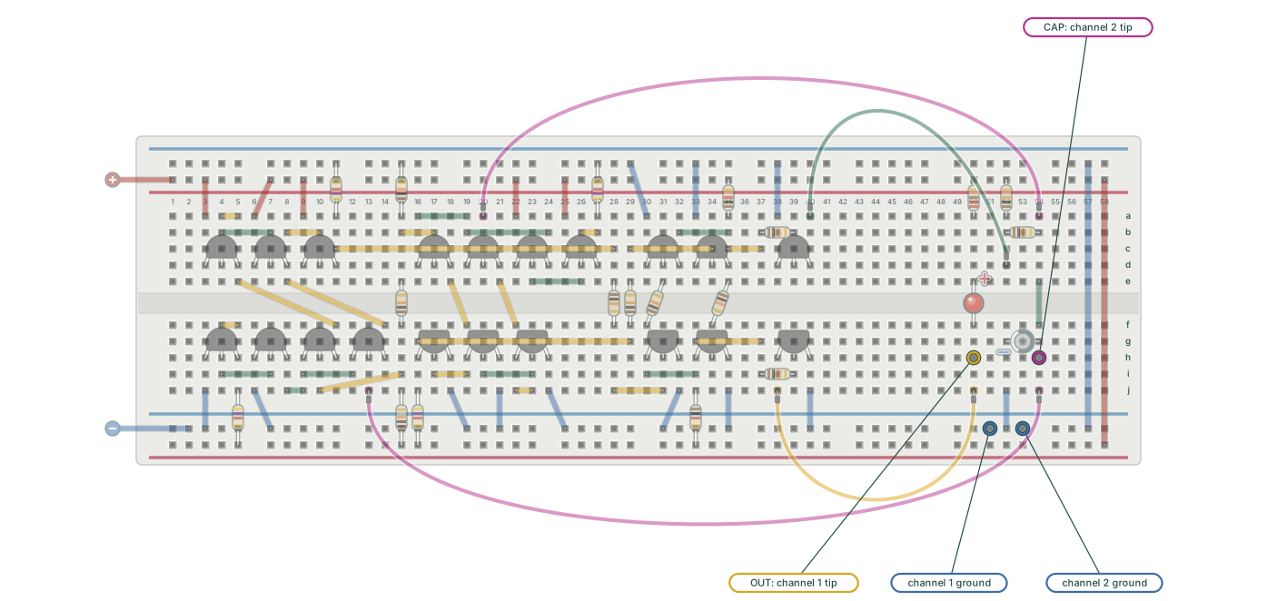
Check that the cursor source is CH2 before you read a turning point. The cursor source is separate from the trigger source, and cursors on the wrong channel read the wrong trace. On my first build of this circuit both turning points read about 0.4 V low, by the same amount. The cursors were on channel 1. The circuit was correct.
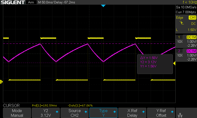
Expect the capacitor trace of Experiment 1: a slow curved rise and a faster fall between about 1.67 V and 3.33 V. OUT is low during the rise and high during the fall. Its high is about 3.6 V, because with Q19 off only the probe's small current flows through the LED. The table compares the expected values with the NE555 of Experiment 1 and with my board.
| Measurement | Expected with nominal parts | NE555, Experiment 1 | My board |
|---|---|---|---|
| Period | About 208 ms | 200.46 ms | 192.59 ms |
| Frequency | About 4.81 Hz | 4.99 Hz | 5.19 Hz |
| LED on | 66.7 % | 66.76 % | 67.06 % |
| CAP minimum | About 1.67 V | 1.68 V | 1.56 V |
| CAP maximum | About 3.33 V | 3.34 V | 3.12 V |
The LED blinks as it blinked on the NE555 in Experiment 1. Twenty transistors on one breadboard now do the work of that chip: Q1 to Q7 in the threshold comparator, Q8 to Q14 in the trigger comparator, Q15 to Q18 in the latch, and Q19 and Q20. Each block came from its own experiment, from the transistor switch of Experiment 3 to the latch of Experiment 11, and each block was tested alone. This experiment connected them, and they run as one timer within 4 % of the NE555's rate.
No block on the board keeps time. The comparators compare, the latch holds one bit and Q20 switches. C sets the time, because its voltage takes time to change.
The divider sets the two turning points. CAP turns at about 1/3 and 2/3 of the supply, because each comparator compares it with a tap of the divider. My board turned at 1.56 V and 3.12 V. That is 0.12 V and 0.22 V below the NE555's 1.68 V and 3.34 V. Possible causes are the comparators' offsets and the divider's resistor tolerances. This experiment does not measure them separately.
RA, RB and C set the time between the turning points. The charge runs through RA and RB, 20 kΩ, and the discharge through RB alone, 10 kΩ. So the charge takes twice as long, and the LED is on for two-thirds of each period. The box “Where the 208 ms comes from” calculates the two times.
During the charge, CAP moves towards 5 V through RA + RB. Call the difference between the supply and CAP the gap. The charge starts with CAP at 1/3 of the supply, so the gap is 2/3 of the supply. It ends at 2/3, where the gap is 1/3. So the gap halves. Experiment 9 showed that the gap halves in 0.69 RC, whatever its size. The charge takes 0.69 × 20 kΩ × 10 µF = 139 ms.
During the discharge, Q20 holds DIS near 0 V, and CAP moves towards 0 V through RB alone. It falls from 2/3 of the supply to 1/3, so it halves too. The discharge takes 0.69 × 10 kΩ × 10 µF = 69 ms. One period is 139 ms + 69 ms = 208 ms, so the rate is 4.81 Hz, and the LED is on for 139 of every 208 ms, two-thirds.
Each time is one halving, and one halving takes times the time constant of its resistance and C:
Add the two times to get the period:
The frequency is one divided by the period. With , one divided by is about 1.44:
The share of the period that the LED is on is the charge time divided by the period. The and the cancel:
My board ran at 5.19 Hz, 8 % above the 4.81 Hz that the nominal parts give. The NE555 ran 4 % above it. Experiment 1 named the causes that can move a rate by that much. They are the tolerances of the resistors and the capacitor, the switching levels and the measurement. On my board the turning points also add to the difference. They are 1.56 V apart, and the NE555's are 1.66 V apart.
The calculation in the box “Where the 208 ms comes from” used only fractions of the supply. Experiment 9 showed that the taps keep their fractions when the supply changes. Experiment 9 also calculated that the time to climb from 1/3 to 2/3 of the supply stays the same at 4.50 V. That is the ratiometric property. On this board it is a measurement.
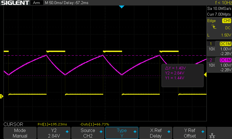
At 4.50 V, CAP has less voltage to cover between the two turning points. C also charges towards a lower supply, so it charges more slowly. By calculation the two changes cancel, so the rate depends only on RA, RB and C. On my board the turning points moved from 1.56 V and 3.12 V to 1.44 V and 2.84 V. The period changed from 192.59 ms to 195.23 ms, by 1.4 %, while the supply changed by 10 %. The LED is a little dimmer, because its current falls to about 11 mA.
The same astable circuit now runs on three builds. Experiment 1 used the NE555, and Experiment 2 used catalogue chips. This experiment uses discrete transistors. Figure 12-10 shows the three captures with the same timebase, 50 ms/div.
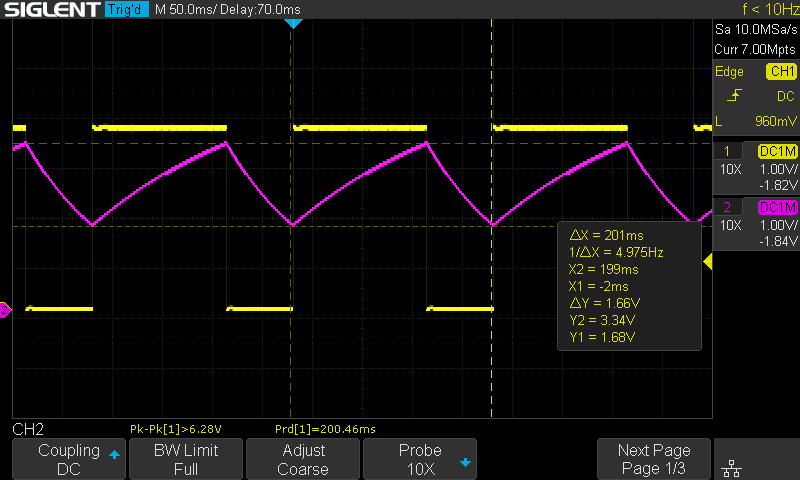
NE555, Experiment 1: 200.46 ms
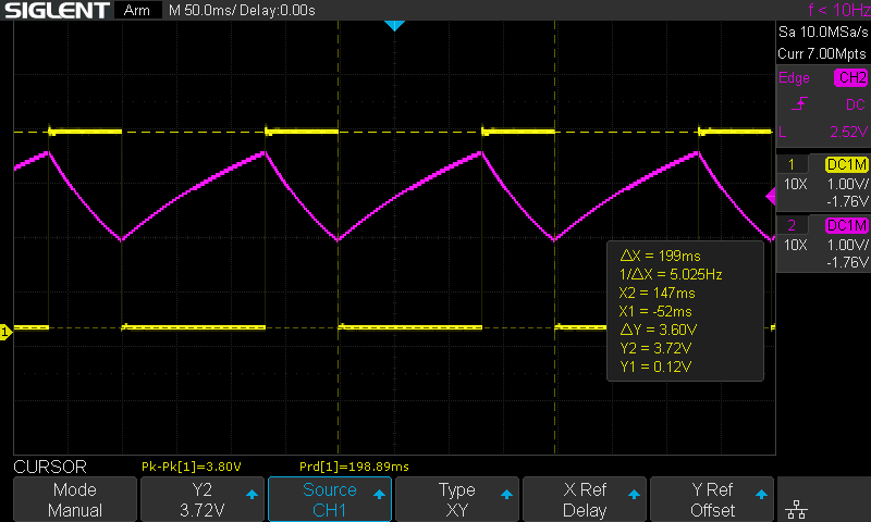
LM393 and CD4001B, Experiment 2: 198.89 ms
Twenty transistors, this experiment: 192.59 ms
The table gives the rate of each, as I measured them.
| Build | Rate |
|---|---|
| NE555 (Experiment 1) | 4.99 Hz |
| LM393 and CD4001B, with the output driver (Experiment 2) | About 5.02 Hz |
| Discrete transistors (this experiment) | 5.19 Hz |
| Formula, 10 kΩ, 10 kΩ and 10 µF | 4.81 Hz |
The three builds agree within about 4 %. The comparison covers the astable rate with an LED load. Other modes and other loads need their own measurements.
Three questions on this experiment. They ask what holds the timer between the turning points, why the charge takes longer, and how the timer starts.
1. CAP is halfway up its rise, and both comparators' OUTs are 0. C continues to charge because…
S and R are both 0, which is the hold state of Experiment 11. The last pulse was on S, so Q stays at 1 and Q̄ at 0. Q20 stays off, and the current through RA and RB continues into C.
2. The charge takes about twice as long as the discharge, because…
Each phase halves a gap, and a halving takes 0.69 times the resistance times C. The charge has twice the resistance of the discharge, so it takes twice the time: 139 ms against 69 ms.
3. At switch-on, C is empty. The LED lights at once, because…
0 V is below the 1/3 tap. The trigger comparator detects that, S sets the latch, and Q turns Q19 on. Q̄ keeps Q20 off, so C starts to charge.
The board runs as a 555 astable, built from twenty transistors and tested block by block. The comparators drive S and R, the latch drives Q19 and Q20, and C drives the comparators. Q19 lights the LED while C charges, and Q20 discharges C through RB. All of it stays on the board. The NE555 has one more input, pin 4, RESET. A low on RESET stops the timer, whatever the capacitor does. Experiment 13: The Reset Pin adds that input to the board.