Full Stack Electronics · Stage Three · Experiment 11
Build the second NOR gate and connect the two gates in a loop. Then drive it from the function generator, and watch it set, hold and reset.
Experiment 10 built one NOR gate from Q15 and Q16. Its OUT follows its inputs at every moment, so it cannot store anything. The timer must store one fact. After the trigger comparator's OUT falls, the capacitor must keep charging until the threshold comparator's OUT rises at 2/3 of the supply. So the timer needs a circuit that records which of the two comparators was high last.
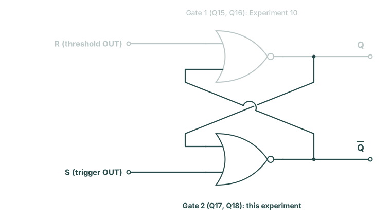
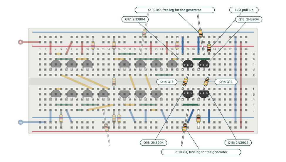
In Experiment 2 that circuit was a latch made from the two NOR gates of a CD4001B chip. This experiment builds the second gate from Q17 and Q18. Then it connects the OUT of each gate to an input of the other gate. The pair then keeps its state after the input that set it returns to 0. Figure 11-1 shows the parts that this experiment adds, in colour.
The latch needs a second gate, and Gate 2 is a copy of the gate from Experiment 10. Q18 and Q17 share a 1 kΩ pull-up and an output, and each one has a 10 kΩ into its base. Two connections make the loop. Each one takes the output of one gate, through a 10 kΩ, to an input of the other gate. Figure 11-2 shows the result. In it, Q16 and Q17 are drawn turned round, with the base on the right. Their inputs then come in from the outputs.
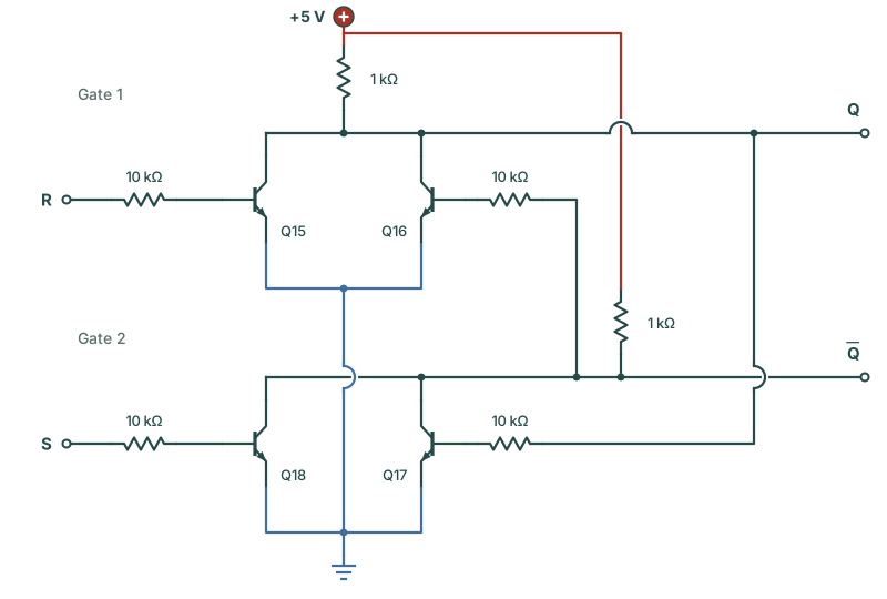
The two inputs that stay free get new names. R, the reset input, goes to Q15, where input A was in Experiment 10. S, the set input, goes to Q18. The output of Gate 1 is called Q, and the output of Gate 2 is called Q̄, said “Q-bar”. The bar means “the opposite of Q”: in normal use one output is 1 and the other is 0. In Experiment 12 the threshold comparator's OUT drives R, and the trigger comparator's OUT drives S. In this experiment, the function generator drives the free leg of each input's 10 kΩ. 0 V gives a 0, and 5 V gives a 1.
The loop gives each gate one input from the other gate. Each gate still follows the NOR rule from Experiment 10: its output is 1 only when both of its inputs are 0. Figure 11-3 shows the latch while S is at 1, and below it again after S returns to 0. A transistor that is off is pale, and green arrows show where current flows. The list gives the reason for each change, in order.
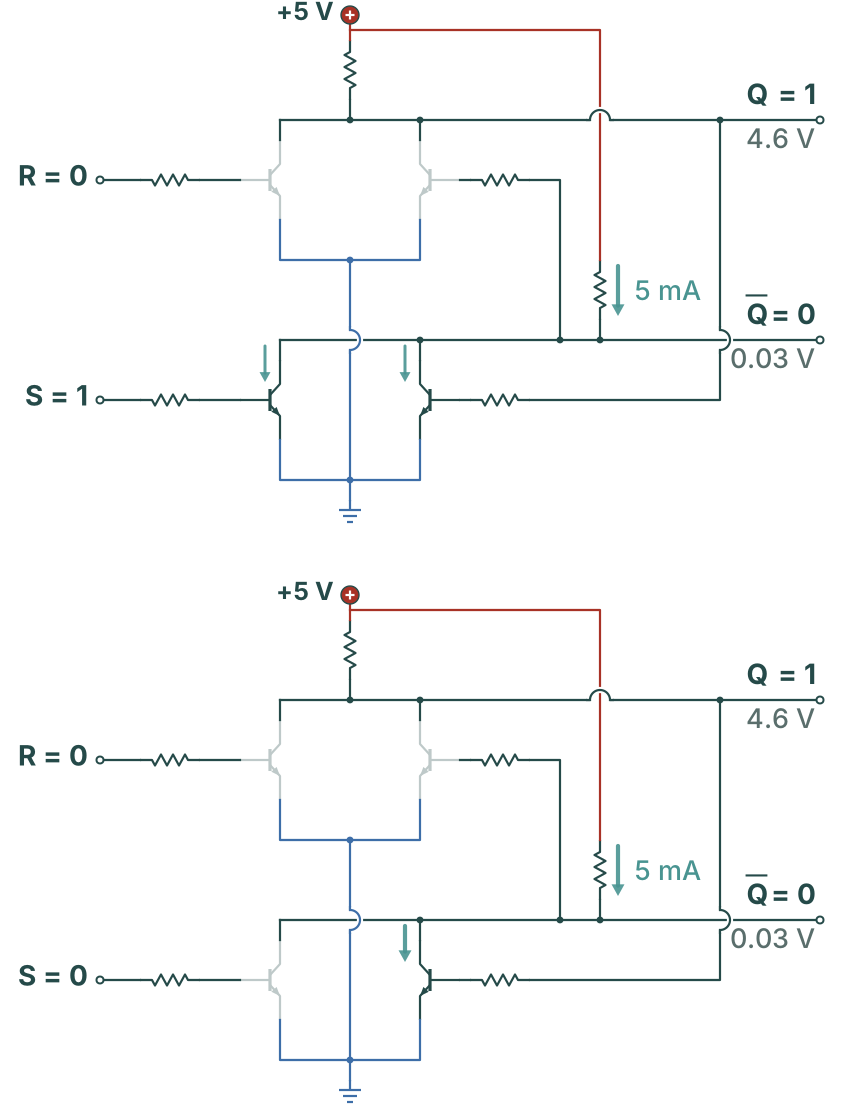
In the lower panel no input is at 1, and Q is still 1. Q holds Q17 on, and Q17 holds Q̄ at 0. Q̄ at 0 lets Gate 1 keep Q at 1. Each output keeps the other gate in its state, so the latch stays set until R changes it.
While the latch is set, a second pulse on S changes nothing, because Q̄ is already 0. In the timer, S comes from the trigger comparator's OUT. If noise makes that OUT rise twice, only the first rise changes the latch.
Figure 11-4 shows the same two steps for R.
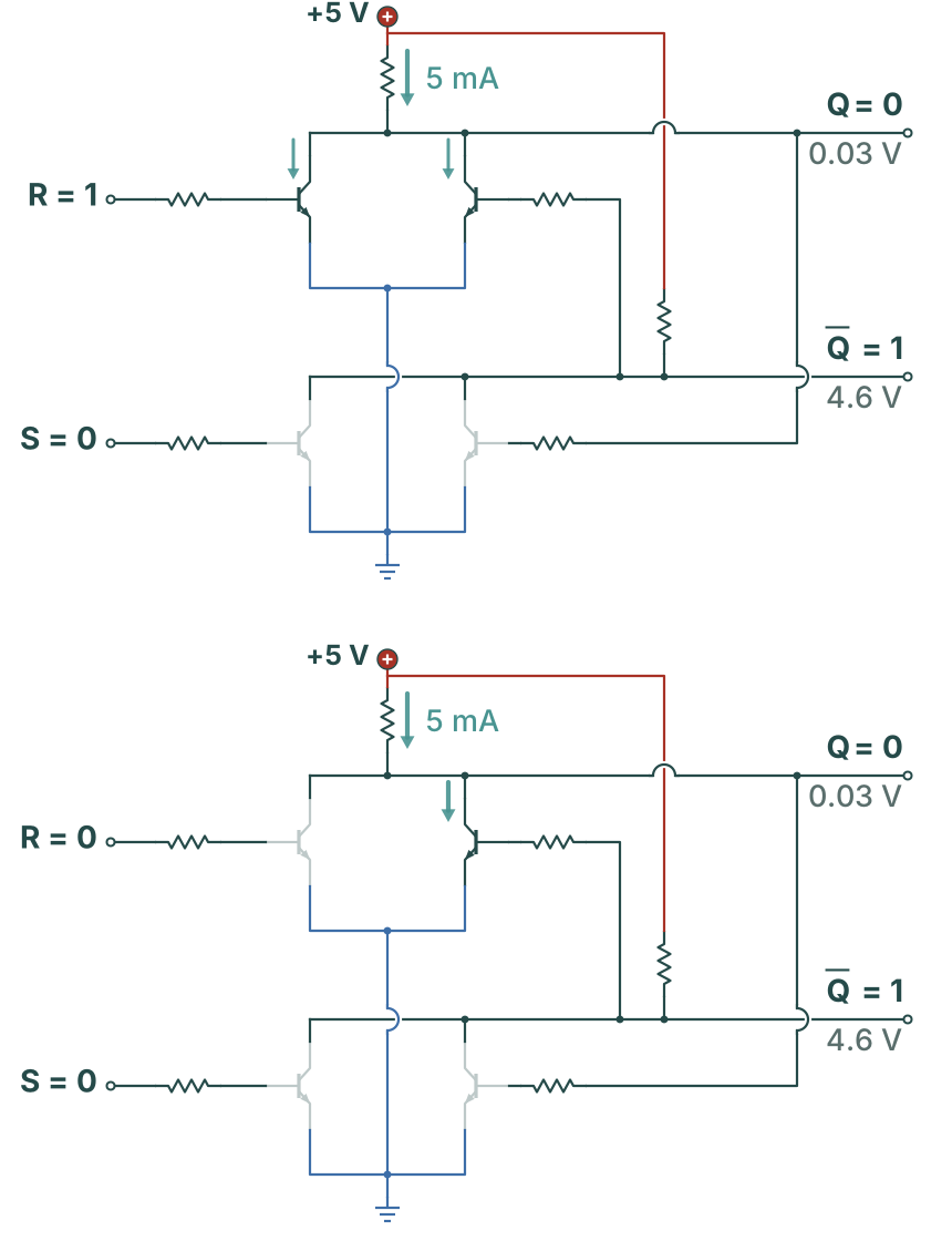
Compare the lower panels of Figures 11-3 and 11-4. In both, S and R are 0. In Figure 11-3 Q is 1, and in Figure 11-4 Q is 0. The inputs are the same and the outputs are opposite, because the latch records which input was 1 last. That record is the one bit of memory that the timer needs.
Figures 11-3 and 11-4 showed how the loop stores one bit. Gate 2 goes in the upper block, straight above Gate 1, in the same columns 28 to 33. In this block the outer top rail is ground and the inner top rail is +5 V. So Q17 and Q18 stand in row d with their flat faces towards the near edge. Their emitters go up to the outer top rail, and their pull-up goes to the inner top rail.
Two new 10 kΩ resistors connect the gates. Each one crosses the channel one column skewed. One brings Q, the lower strip of column 28, to Q17's base in column 29. The other brings Q̄, the upper strip of column 33, to Q16's base in column 32. Input B's 10 kΩ comes out, because Q16's base now takes Q̄.
The function generator drives both inputs of the latch, so neither input resistor goes in a rail. R is input A of Experiment 10. Its 10 kΩ already stands in 29j with its free leg over the bottom rails, as the oscilloscope test of Experiment 10 left it. S's 10 kΩ stands in Q18's base strip at 32a, with its free leg over the top rails. Figure 11-5 shows the finished latch.
The latch is complete. The two channels of the function generator take the place of the two comparators. Channel 1 drives S with a 1 ms pulse every 10 ms. Channel 2 drives R with the same pulse, 5 ms later. Oscilloscope channel 1 shows S, through a BNC T-piece on generator channel 1. Channel 2 shows Q, and channel 3 shows Q̄. R is not on the oscilloscope: Q falls at the start of each R pulse, so Q shows where R is. Figure 11-6 shows the connections.
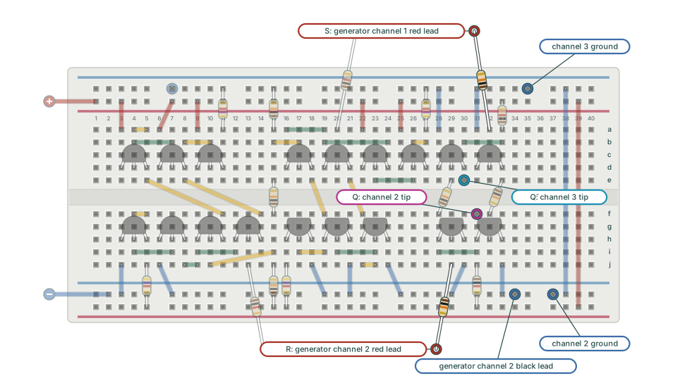
Before you read a level, make sure that each channel's probe setting agrees with its probe. A ×10 probe on a channel set to ×1 shows one tenth of the voltage. A 1 at 4.6 V then reads 0.46 V and looks like a 0. On my first build of this latch, one output seemed to stay at 0 for this reason. The circuit was correct.
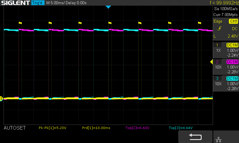
Q rises at the start of each S pulse. The S pulse ends 1 ms later, and Q stays at 1 for the next 4 ms, while S and R are both 0. Then the R pulse resets the latch, and Q stays at 0 until the next S pulse. So Q is high for 5 ms in each 10 ms. Q̄ is the opposite of Q all the time. The table gives the four states in each 10 ms period, with the expected levels.
| State | Time | S | R | Q | Q̄ |
|---|---|---|---|---|---|
| Set | 0 to 1 ms | 1 | 0 | 4.6 V | 0.03 V |
| Hold after set | 1 to 5 ms | 0 | 0 | 4.6 V | 0.03 V |
| Reset | 5 to 6 ms | 0 | 1 | 0.03 V | 4.6 V |
| Hold after reset | 6 to 10 ms | 0 | 0 | 0.03 V | 4.6 V |
The two hold rows have the same inputs and opposite outputs. The difference is the bit that the loop stores. On my current board the Top measurements in Figure 11-7 read 4.60 V on Q and 4.64 V on Q̄. The section “Why the high is 4.6 V” explains why it is lower than in Experiment 10.
If Q follows S and falls as soon as the S pulse ends, check the two 10 kΩ resistors across the centre channel. One must go from 28f to 29e, and the other from 33e to 32f. If an output shows a slow wave of a few tenths of a volt where a 1 must be, that output is not connected. Check that each lead is tight in its clip, and that each pull-up is in its +5 V rail.
The time from an S pulse to the next R pulse sets how long Q stays high.
In the timer, the capacitor sets that time. S rises when the capacitor voltage falls below 1/3 of the supply, and R rises when it passes 2/3. The latch holds Q at 1 while the capacitor charges from one level to the other.
The table expects a 1 of about 4.6 V on both outputs. In Experiment 10 a 1 at OUT read 5.003 V on my current board, but there OUT drove only the multimeter. In the latch, Q also drives Q17's base through a 10 kΩ, and the current for that base flows through the pull-up of Gate 1. Figure 11-8 shows that path while the latch holds the set state.
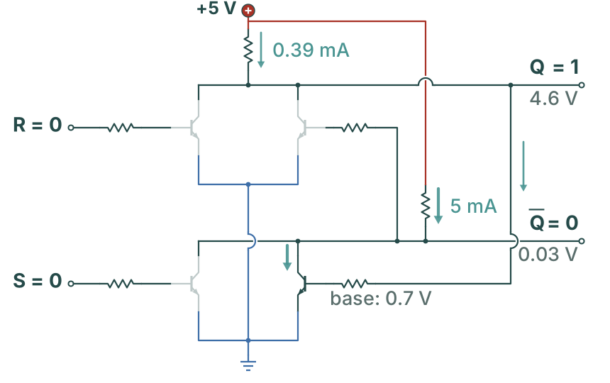
In the reset state Q̄ drives Q16 in the same way, so a 1 on Q̄ is also about 4.6 V. That is still far above the band from 0.60 V to 1.10 V where a transistor switch from Experiment 3 changes state. The 0.39 mA into Q17's base is more than five times the 0.07 mA that its 5 mA collector current needs. So the 0 on Q̄ stays near 0.03 V.
Each further input on Q takes its own base current through the same 1 kΩ, and the 1 falls again. This is a weak point of resistor-transistor logic: one output can drive only a few inputs. Experiment 12 connects more inputs to Q and Q̄, so it must keep their base currents small.
The pulses so far never put S and R at 1 at the same time. Figure 11-9 shows what happens then.
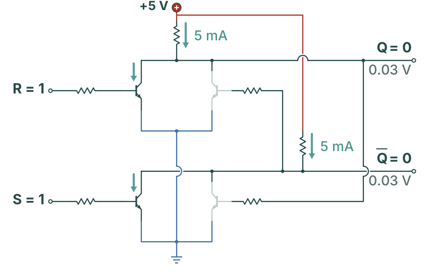
Each gate has one input at 1, so both outputs are 0. Q and Q̄ are then the same, and the bar no longer means “the opposite of Q”. The next state depends on the input that returns to 0 last. If S returns to 0 first, R is still 1 and resets the latch. If R returns to 0 first, S sets it. If both return to 0 at the same moment, both outputs start to rise together. Small differences between the transistors then decide the state, so nobody can say in advance which state follows.
Wider pulses that overlap show this on the oscilloscope. S rises first, and R rises 1 ms later. S also falls first, so R resets the latch.
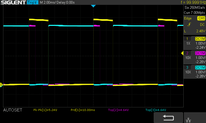
S sets the latch at 0 ms, and Q rises. At 1 ms R rises too. Both outputs are then 0, so neither trace is high. At 3 ms S falls while R is still 1, so Q̄ rises and the latch is reset. When R falls at 4 ms, Q stays at 0. On my current board the oscilloscope measured Q high for 1 ms in each 10 ms, and Q̄ low for 3.00 ms.
The timer never puts S and R at 1 together. Experiment 9 showed that the trigger comparator's OUT is high only while the ramp is below 1/3 of the supply. The threshold comparator's OUT is high only while the ramp is above 2/3. In Experiment 12 one capacitor voltage drives both comparators, and it cannot be below 1/3 and above 2/3 at the same time.
The NE555 has a latch at the same place. The Texas Instruments datasheet for the NE555 (SLFS022K) describes it. A trigger voltage below 1/3 of the supply sets the latch, and a threshold voltage above 2/3 resets it. Its function table also gives the case with both at once. With the trigger below 1/3, the output is high, whatever the threshold voltage is. So in the chip, S has priority over R.
The latch in this experiment has no priority, and both of its outputs go to 0. In a timer where one capacitor drives both pins, the case does not occur. It can occur when a circuit outside the chip drives the trigger pin. Then a trigger pulse that lasts longer than the timing period keeps the output high until the pulse ends.
In 1918 William Eccles and Frank Jordan, two physicists in London, filed a British patent. Their circuit had two vacuum tubes. The output of each tube drove the input of the other tube, as Q and Q̄ do in this latch. A pulse changed its state, and the state then stayed. They published the circuit in 1919 as a “trigger relay”. About twenty years later, the same circuit stored bits in Colossus and ENIAC, two of the first electronic computers.
Three questions on this experiment. They ask about the hold state, what keeps the latch in its state, and why its 1 is lower than in Experiment 10.
1. With S and R both at 0, Q…
S = 0 and R = 0 is the hold state. Each output keeps the other gate in its state. So Q stays at 1 after a pulse on S, and at 0 after a pulse on R.
2. After S returns to 0, Q17 stays on because…
Q stays at 1 while Q̄ is 0, and Q drives about 0.39 mA into Q17's base. Q17 then keeps Q̄ at 0. Without the 10 kΩ from 28f to 29e, the latch loses its state as soon as S returns to 0.
3. A 1 in the latch is about 4.6 V, lower than the 5.003 V of Experiment 10, because…
About 0.39 mA flows from +5 V through the 1 kΩ and the 10 kΩ into the next gate's base. It puts about 0.39 V across the 1 kΩ, so the 1 sits at about 4.6 V.
Two NOR gates, with the output of each on an input of the other, make an SR latch. A pulse on S sets Q to 1, and a pulse on R resets it to 0. With both inputs at 0, the latch holds its last state. Its 1 is about 4.6 V and its 0 about 0.03 V. The latch stays on the board, in columns 28 to 33, Gate 2 above Gate 1.
The board now holds every block of the timer: two comparators, the divider that sets their thresholds, and the latch. Experiment 12: The Swap connects the trigger comparator's OUT to S and the threshold comparator's OUT to R. It adds the timing resistors and capacitor and two more transistors, and the board then runs as a timer.